Apparatus and method for a voltage regulator with improved power supply reduction ratio (PSRR) with reduced parasitic capacitance on bias signal lines

a voltage regulator and parasitic capacitance technology, applied in the field of linear voltage regulator circuits, can solve the problems of large capacitance, large noise, and high impedance of bias lines, and achieve the effect of lessening the impact of parasitic capacitan

Active Publication Date: 2017-06-06
DIALOG SEMICONDUCTOR GMBH
View PDF34 Cites 19 Cited by
  • Summary
  • Abstract
  • Description
  • Claims
  • Application Information

AI Technical Summary

Benefits of technology

[0011]A principal object of the present disclosure is to provide a circuit implementation which lessens the impact of parasitic capacitance associated with bias lines.
[0012]A principal object of the present disclosure is to provide a circuit that reduces the impact of parasitic capacitance on power supply rejection ratio (PSRR) of analog functional blocks.
[0013]Another further object of the present disclosure is to provide a circuit device with analog blocks that reduces the standby current for the system.
[0020]The above and other objects are further achieved by a method of improved power supply rejection ratio (PSRR) frequency dependence in a system comprising the steps of providing a system comprising a functional block, a master bias network, an enabling switch, a bias line, and a regulated power supply, feeding a regulated voltage to said enabling switch, feeding a voltage representing a voltage supply to said functional block; and minimizing bias line parasitic capacitance for improved power supply rejection ratio (PSRR) through design layout.
[0021]The above and other objects are further achieved by a method of improved power supply rejection ratio (PSRR) frequency dependence in a system comprising the steps of providing a system comprising a functional block, a master bias network, an enabling switch, a bias line, a low pass filter (LPF) and a regulated power supply, feeding a regulated voltage to said enabling switch, filtering the output of said enable switch using said low pass filter (LPF), and minimizing bias line parasitic capacitance for improved power supply rejection ratio (PSRR) through design layout.

Problems solved by technology

With the reduction of the bias current, leads to bias lines to become high impedance.
Additionally, with the reduction of the bias current, noise has a larger influence.
With the long bias lines on the order of milli-meters, the magnitude of the capacitance, and the noise signal is significant, and impacts the power supply rejection ratio (PSRR).
In a large system, the routing lines can be of significant length leading to power supply reduction ratio (PSRR) degradation.

Method used


Image

  • Apparatus and method for a voltage regulator with improved power supply reduction ratio (PSRR) with reduced parasitic capacitance on bias signal lines
  • Apparatus and method for a voltage regulator with improved power supply reduction ratio (PSRR) with reduced parasitic capacitance on bias signal lines
  • Apparatus and method for a voltage regulator with improved power supply reduction ratio (PSRR) with reduced parasitic capacitance on bias signal lines

Examples


first embodiment

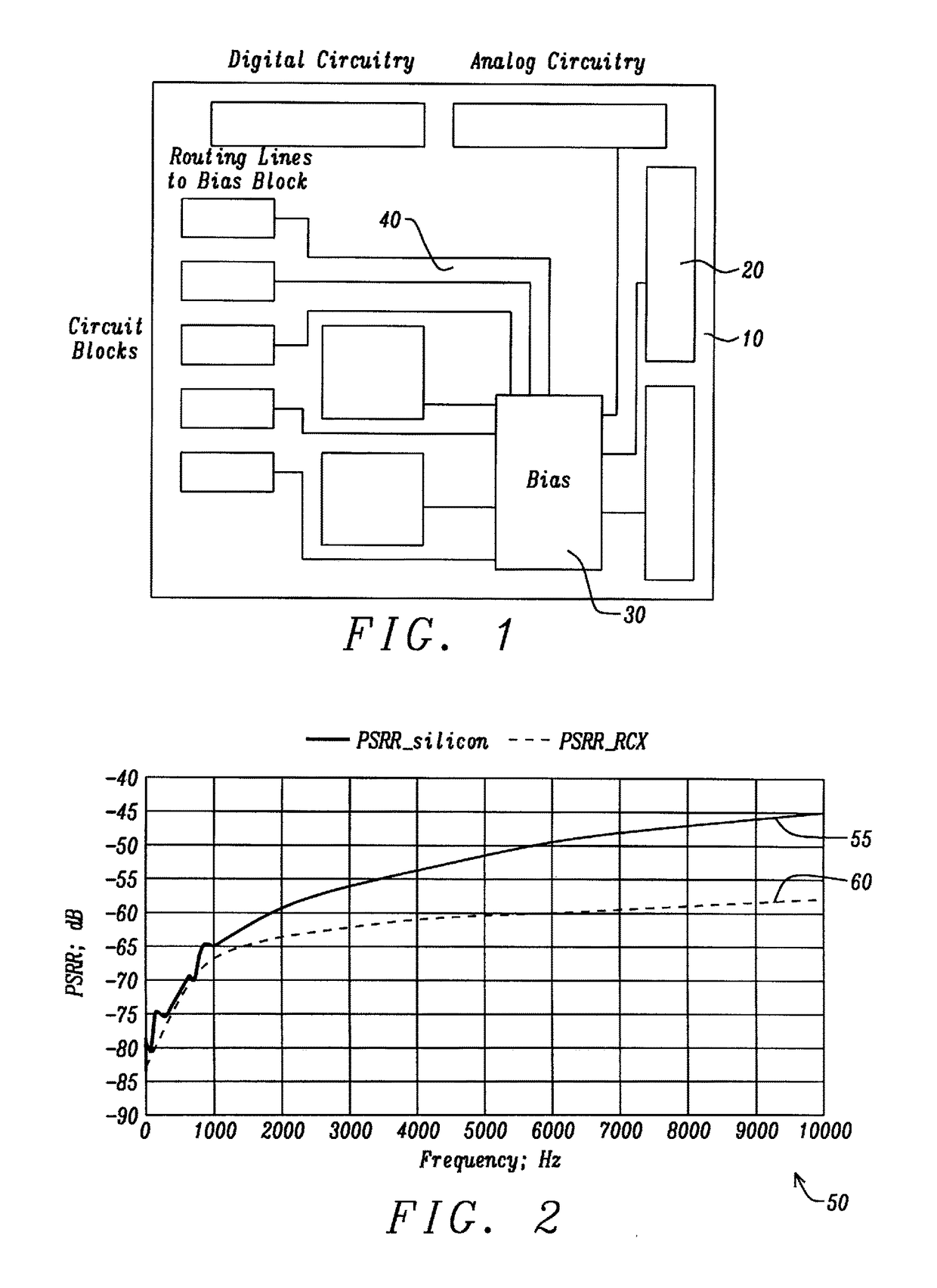
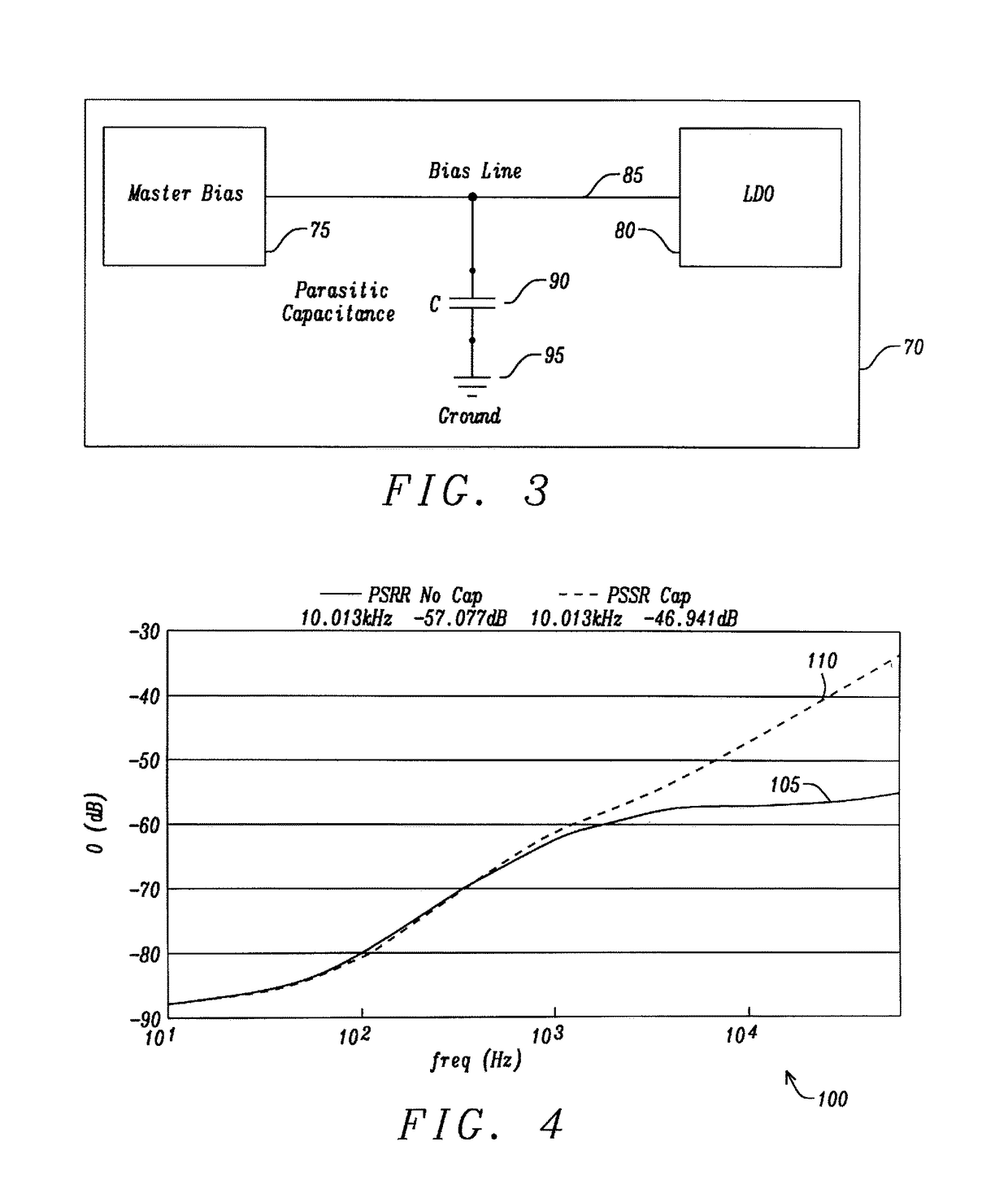
[0040]FIG. 6 is a circuit schematic diagram illustrating the internal connections from the bias current from the bias block to the low drop out (LDO) regulator in accordance with the disclosure. The circuit contains an n-channel MOSFET switch N1120. The n-channel MOSFET switch N1120 enables the flow of bias current to the low dropout (LDO) when the LDO is in an enable mode of operation. The circuit contains a p-channel MOSFET 130 between the battery voltage 135, and the n-channel MOSFET switch N1120. A bias current generator 140 represents the circuit bias between n-channel MOSFET 120 and ground connection 150. A circuit 200 is represented by I1 controls the gate of n-channel MOSFET N1120. The circuit 200 is electrically connected to regulated power supply 210. With the electrical connection to VREG, the circuit utilizes a ripple free / regulated / filtered supply. The ENABLE function enters the network as a input to circuit element 220. Parasitic capacitance associated with n-channel M...

second embodiment

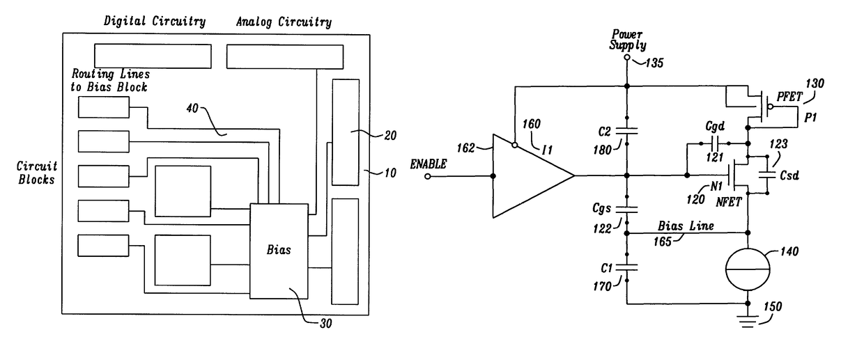
[0043]FIG. 8 is a circuit schematic diagram illustrating the internal connections from the bias current from the bias block to the low drop out (LDO) regulator in accordance with the disclosure. The circuit contains an n-channel MOSFET switch N1120. The n-channel MOSFET switch N1120 enables the flow of bias current to the low dropout (LDO) when the LDO is in an enable mode of operation. The circuit contains a p-channel MOSFET 130 between the battery voltage 135, and the n-channel MOSFET switch N1120. A bias current generator 140 represents the circuit bias between n-channel MOSFET 120 and ground connection 150. A circuit 160 is represented by I1 is electrically connected to the power supply 135. The ENABLE function enters the network as an input to circuit element 162. Parasitic capacitance associated with n-channel MOSFET 120 are gate-to-drain capacitance 121, gate-to-source capacitance 122, and source-to-drain capacitance 123. Parasitic capacitance from the routing line 165 to gro...

fourth embodiment

[0046]FIG. 10 is a circuit schematic diagram illustrating the internal connections from the bias current from the bias block to the low drop out (LDO) regulator in accordance with the disclosure. The circuit contains a p-channel MOSFET switch PFET 310. The p-channel MOSFET switch 310 enables the flow of bias current to the low dropout (LDO) when the LDO is in an enable mode of operation. The circuit contains a bias current network 280 between the battery voltage 135, and the p-channel MOSFET switch 310. A “On MOSFET” NFET N2290 is electrically connected bias between p-channel MOSFET 310 and ground connection 150. A digital gate 220 is represented by I1 which is driven of the LDO supply and controls the gate of p-channel MOSFET 310 and is electrically connected to the regulated voltage supply 300. With the electrical connection to the regulated voltage supply, the circuit utilizes a ripple free / regulated / filtered supply. The ENABLE function enters the network as an input to circuit e...


PUM


Abstract

An apparatus and method for a system with improved power supply rejection ratio (PSRR) over a wide frequency range. The improved PSRR is achieved by negating the influence of the parasitic capacitance associated with the bias lines and the introduction of a regulated power supply with embodiments associated with providing a ripple free and regulated supply. With reduction of parasitic capacitance, and providing an ENABLE switch by a pre-regulated supply, the degradation of the PSRR is achieved. The embodiments include both n-channel and p-channel MOSFETs implementations, and a positive and negative regulated power supply voltage. With the combined influence of the utilization of the VREG supply, and the lowering of battery-to-bias line capacitance using design layout and improved floor planning an improved PSRR over a wide frequency distribution is achieved.

Description

BACKGROUND[0001]Field[0002]The disclosure relates generally to a linear voltage regulator circuits and, more particularly, to a linear voltage regulator circuit device having improved power supply reduction ratio (PSRR) thereof.[0003]Description of the Related Art[0004]Linear voltage regulators are a type of voltage regulators used in conjunction with semiconductor devices, integrated circuit (IC), battery chargers, and other applications. Linear voltage regulators can be used in digital, analog, and power applications to deliver a regulated supply voltage. In power management semiconductor chips, it is desirable to consume the least amount of power possible to extend the battery power. In the initialization of a power management semiconductor chip, a bias current is needed for the internal nodes and branches. This start-up bias current establishes a pre-condition state for many power applications. The bias current magnitude should be a low value to extend battery life. With the red...

Claims


Application Information

Patent Timeline
Patent Type & Authority Patents(United States)
IPC IPC(8): G05F1/563G05F1/575
CPCG05F1/563G05F1/575
Inventor BHATTAD, AMBREESHNIKOLOV, LUDMIL
Owner DIALOG SEMICONDUCTOR GMBH
Why Eureka
Try Eureka