

Direct current superposition freeze
a direct current and superposition freeze technology, applied in the field of thin film patterning and various layers, can solve the problems of limiting the pitch or spacing between exposed features, thermal freezing, and inability to meet the requirements of the application, and achieve the effect of improving the lfle process and improving the roughness of the line edg
- Summary
- Abstract
- Description
- Claims
- Application Information
AI Technical Summary
Benefits of technology
Problems solved by technology
Method used
Image

Examples
Embodiment Construction
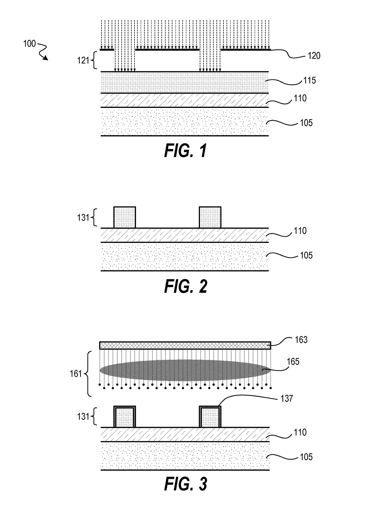
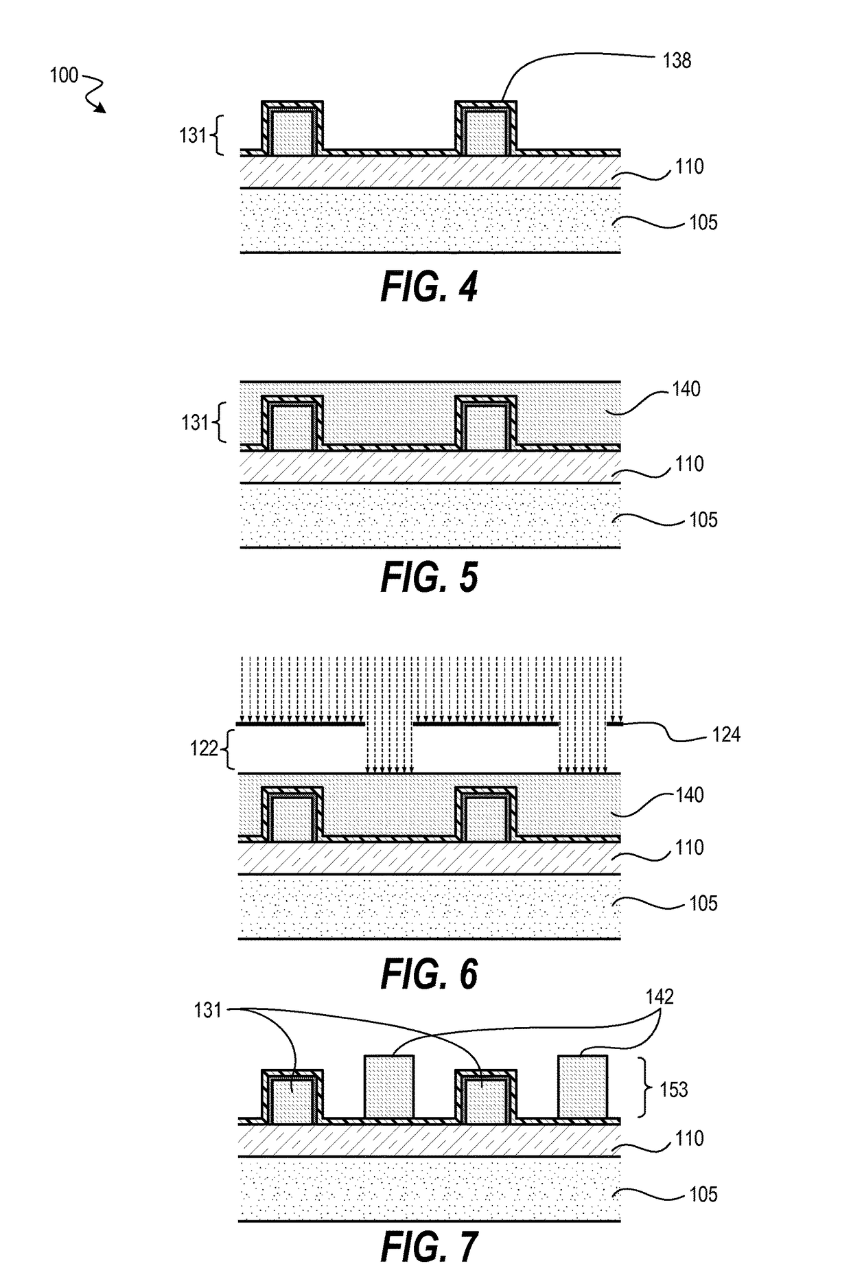
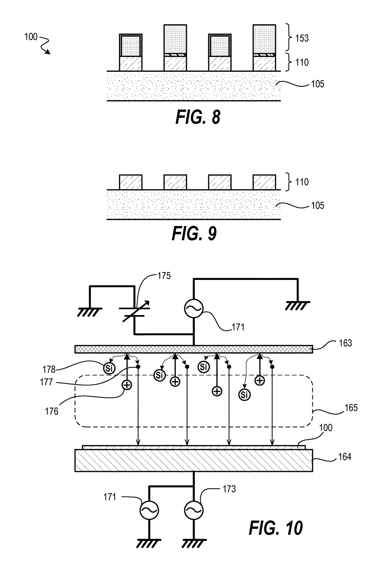
[0018]Systems and methods disclosed herein include improved techniques for patterning substrates, including improvements to double patterning techniques. Techniques herein combine direct current superposition plasma processing with photolithographic patterning techniques. An electron flux or ballistic electron beam herein from plasma processing can induce cross linking in a given photoresist, which alters the photoresist to be resistant to subsequent light exposure and / or developer treatments. Plasma processing can also be used to add a protective layer of oxide on exposed surfaces of a first relief pattern, thereby further protecting the photoresist from a developing acid. By protecting an initial photoresist relief pattern from developing acid, a second pattern can be applied on and / or between the first photoresist relief pattern thereby doubling an initial pattern or otherwise increasing pattern density. This combined pattern can then be used for subsequent processing such as tra...
PUM
| Property | Measurement | Unit |
|---|---|---|
| frequencies | aaaaa | aaaaa |
| frequencies | aaaaa | aaaaa |
| DC voltage | aaaaa | aaaaa |
Abstract
Description
Claims
Application Information