Method of manufacturing thin film transistor, thin film transistor manufactured by the method, and electronic device comprising the thin film transistor

a manufacturing method and technology of a thin film transistor, applied in the direction of sustainable manufacturing/processing, climate sustainability, semiconductor devices, etc., can solve the problem of easy and achieve the effect of reducing or minimizing damage to organic semiconductors and improving tact tim

Active Publication Date: 2017-09-12
SAMSUNG ELECTRONICS CO LTD
View PDF12 Cites 1 Cited by
  • Summary
  • Abstract
  • Description
  • Claims
  • Application Information

AI Technical Summary

Benefits of technology

[0011]Example embodiments provide a method of manufacturing a thin film transistor capable of improving a tact time and reducing or minimizing damage to an organic semiconductor during processes.

Problems solved by technology

However, because the organic semiconductor may be more easily damaged due to the characteristics of the organic material during subsequent processes, the organic material is required to be protected from the subsequent processes by forming a protective layer thereon the organic semiconductor.

Method used


Image

  • Method of manufacturing thin film transistor, thin film transistor manufactured by the method, and electronic device comprising the thin film transistor
  • Method of manufacturing thin film transistor, thin film transistor manufactured by the method, and electronic device comprising the thin film transistor
  • Method of manufacturing thin film transistor, thin film transistor manufactured by the method, and electronic device comprising the thin film transistor

Examples


example

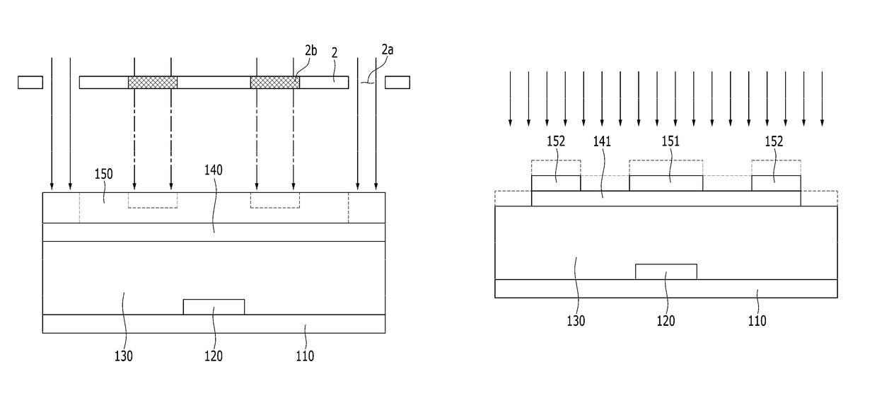
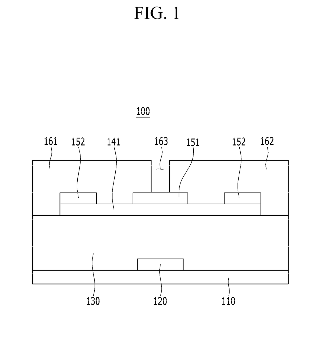
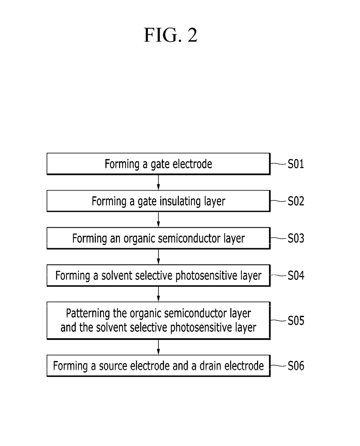
[0115]A gate electrode is formed by sputtering molybdenum on a glass substrate and treating it through photolithography. Subsequently, a gate insulating layer is formed by depositing silicon oxide in a chemical vapor deposition (CVD) method. On the surface of the gate insulating layer, a self-assembled layer is formed by using octadecyltrichlorosilane. Subsequently, a heteroacene-based organic semiconductor represented by Chemical Formula 4 is vacuum-deposited to form an organic semiconductor thin film.

[0116]

[0117]Subsequently, a fluorine-containing photosensitive layer is formed by coating a composition including ethoxynonafluorobutane (C4F9OC2H5, 3M™NoVec™ Co.), a photo acid generator, and a fluorine-containing solvent, and a solvent selectivity photosensitive layer is exposed by using a halftone mask and radiating 365 nm (i-line) light having energy of 50 mJ / cm2 and developed. Then, O2 plasma of 100 sccm and 75 mTorr is applied under a condition of 300 W for 30 seconds to the par...


PUM


Abstract

A method of manufacturing a thin film transistor includes forming a gate electrode, forming a gate insulating layer on the gate electrode, forming an organic semiconductor layer on the gate insulating layer, forming a solvent selective photosensitive layer on the organic semiconductor layer, forming an organic semiconductor pattern and a solvent selective photosensitive pattern by simultaneously patterning the organic semiconductor layer and the solvent selective photosensitive layer, respectively, and forming a source electrode and a drain electrode on the organic semiconductor pattern and the solvent selective photosensitive pattern, the source electrode and the drain electrode being electrically connected to the organic semiconductor pattern.

Description

CROSS REFERENCE TO RELATED APPLICATION[0001]This application claims priority to and the benefit of Korean Patent Application No. 10-2015-0191451 filed in the Korean Intellectual Property Office on Dec. 31, 2015, the entire contents of which are incorporated herein by reference.BACKGROUND[0002]1. Field[0003]Example embodiments relate to a method of manufacturing a thin film transistor, a thin film transistor manufactured according to the method, and an electronic device including the same.[0004]2. Description of the Related Art[0005]A flat panel display, e.g., a liquid crystal display (LCD), an organic light emitting diode (OLED) display, an electrophoretic display, etc., includes a pair of electric field-generating electrodes and an electrical optical active layer interposed therebetween. The liquid crystal display (LCD) includes a liquid crystal layer as an electric optical active layer, and the organic light emitting diode (OLED) display includes an organic emission layer as an el...

Claims


Application Information

Patent Timeline
Patent Type & Authority Patents(United States)
IPC IPC(8): H01L51/05H01L27/28H01L51/00
CPCH01L51/0545H01L27/283H01L51/0017H01L51/0018H01L51/0074H01L51/0558Y02P70/50H10K19/10H10K71/233H10K85/6576H10K10/484H10K10/466H10K71/231
Inventor YUN, YOUNGJUNKIM, JOO YOUNGSONG, BYONG GWONJANG, JAEWONJUNG, JIYOUNGCHOI, AJEONG
Owner SAMSUNG ELECTRONICS CO LTD
Why Eureka
Try Eureka