Bent optical waveguide

a waveguide and optical technology, applied in the field of optical and photonics, can solve the problems of preventing the realization of advanced waveguide circuits, and limiting the ‘bandwidthdistance’ product of multi-mode waveguides, etc., and achieves the effect of improving and tightening the bend

Active Publication Date: 2017-10-03
TEKNOLOGIAN TUTKIMUSKESKUS VTT
View PDF14 Cites 9 Cited by
  • Summary
  • Abstract
  • Description
  • Claims
  • Application Information

AI Technical Summary

Benefits of technology

[0025]The utility of the suggested solution arises from multiple issues depending on the embodiment. For example, ultra-small bends with low losses in micron-scale HIC multimode waveguides may be obtained. Both matched and generic (unmatched) bends with varying curvature may be capitalized. The applicable bandwidth may be considerably large. The designed bends feature minimal bending radii comparable to the waveguide width. Experimental results further confirm the overall effectiveness, robustness and low losses of the realized bends. As an outcome, the ‘footprint’, i.e. the occupied surface area, and cost of the associated circuits are reduced and previously unaffordable elements may become feasible.
[0026]For example, the size of multi-mode interferometric reflectors may be remarkably shrunk. On the other hand, bends with larger radii and lower losses may be used, for example, to design long spirals with low footprint. E.g. an area of about 0.5×0.5 mm2 could somewhat easily allocate an 8 cm long spiral. The proposed bends are also expected to enable the fabrication of microring resonators with high finesse. Various embodiments of the present invention are suitable for use with SOI (silicon-on-insulator) platforms including thicker SOIs and interfaceable with optical fibres. Micron-scale features of the proposed designs allow for fabrication with relaxed lithographic resolution by tools that are much less expensive than the ones usually needed for scalable production of nanophotonic devices. High confinement of light in multi-mode HIC waveguides makes the proposed solution much less sensitive to fabrication errors, wavelength changes and mode polarization than the existing nanophotonic counterparts.
[0027]Generally, waveguides with small birefringence, good fiber coupling, and robustness to fabrication errors, may be obtained in contrast to e.g. fixed curvature bends and / or nanophotonic waveguides.

Problems solved by technology

However, multimode distortion limits the ‘bandwidth×distance’ product of multi-mode waveguides in contrast to single-mode solutions.
It also complicates (or prevents) the realization of advanced waveguide circuits that densely integrate a large number of waveguide components (couplers, filters etc.).
Sub-micron waveguides could be utilized for achieving dense integration, but they pose many additional challenges, including polarization dependence and low coupling efficiency to optical fibre modes.
Furthermore, for scalable production they require expensive state-of-the-art fabrication tools in order to resolve submicron features and are also very sensitive to nanometer-scale fabrication errors.
However, in practice this has led to the inevitable excitation of HOMs if the bending radius has been reduced by a factor of 10 or more with respect to the corresponding low-loss rib waveguide bend.
Nevertheless, the obtained bending radii are still relatively large, in practice e.g. two orders of magnitude larger than the waveguide width, and in particular, manufacturing thereof is challenging due to very stringent tolerance requirements.

Method used


Image

  • Bent optical waveguide
  • Bent optical waveguide
  • Bent optical waveguide

Examples


Embodiment Construction

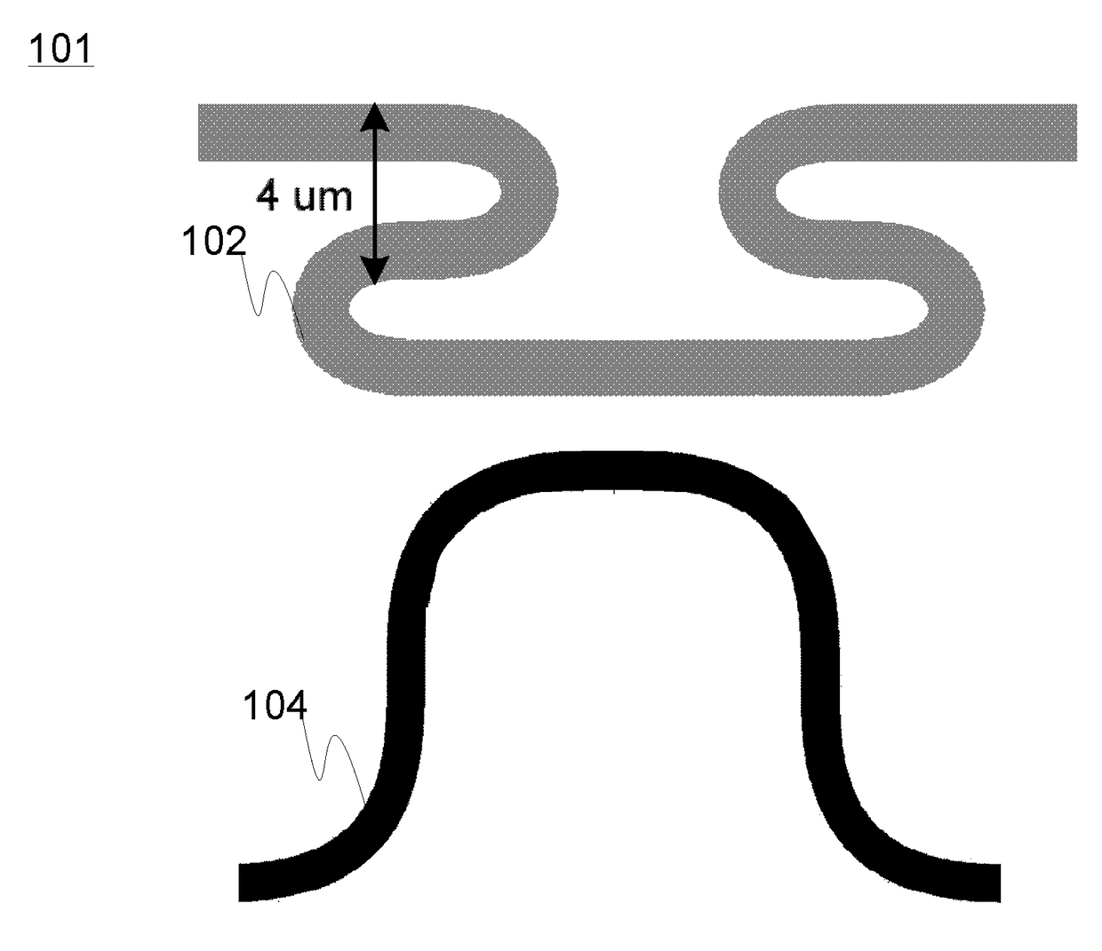
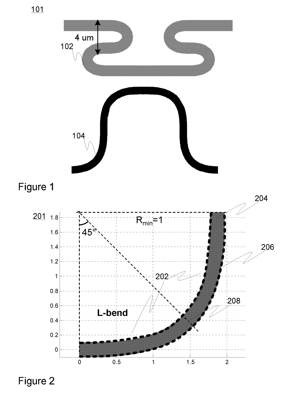
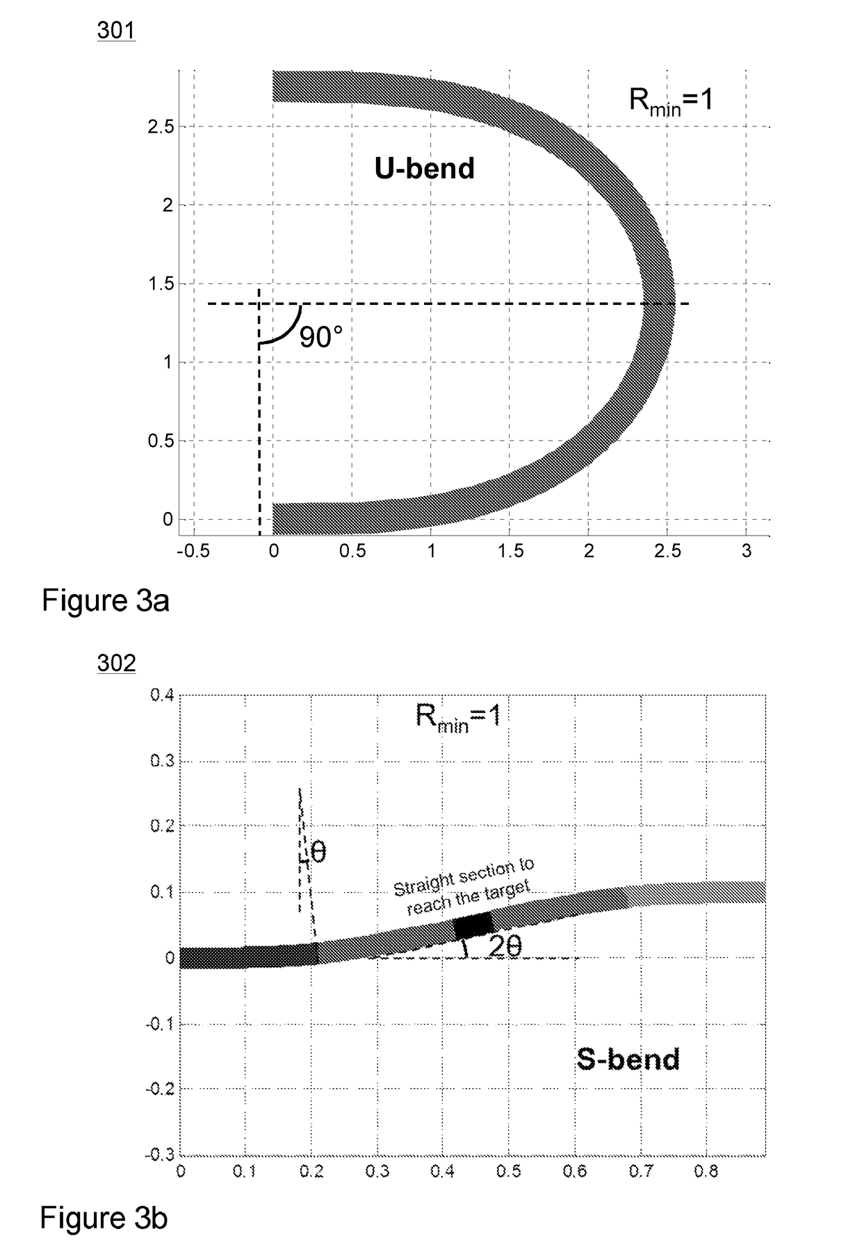
[0046]In FIG. 1 at 101, by way of example only, two different embodiments of the present invention are generally illustrated at 102 and 104. Bends such as ‘U’-bends, ‘S’-bends, ‘U’-bends and practically any bend of a desired degree may be manufactured. Different basic bend shapes may be cleverly combined to establish more complex bends and (mirror / point) symmetry may be exploited to design the bends.

[0047]For instance, two ‘U’-bends could be combined to form an ‘S’-bend, and the ‘U’-bend itself could be constructed from two mirror-symmetric halves, i.e. doubly symmetric structures could be established. However, a skilled reader will understand such symmetry is not obligatory for utilizing the present invention to establish bends, i.e. the bend portions preceding and following e.g. the point of maximum curvature of a bend do not have to be mirror-symmetric.

[0048]The obtained bends are optically efficient and provide small footprint due to optimized, yet small, non-constant bend radii...


PUM


Abstract

An optical multi-mode HIC (high index contrast) waveguide (102, 104, 201, 301) for transporting electromagnetic radiation in the optical waveband, the waveguide comprising a guiding core portion (204) with higher refractive index, and cladding portion (206) with substantially lower refractive index configured to at least partially surround the light guiding core in the transverse direction to facilitate confining the propagating radiation within the core, the waveguide being configured to support multiple optical modes of the propagating radiation, wherein the waveguide incorporates a bent waveguide section (202) having bend curvature that is configured to at least gradually, preferably substantially continuously, increase towards a maximum curvature of said section from a section end.

Description

FIELD OF THE INVENTION[0001]Generally the present invention relates to optics and photonics. In particular, however not exclusively, the present invention concerns HIC (high index contrast) optical multi-mode waveguides and bending thereof.BACKGROUND[0002]Optical waveguides including multi-mode dielectric waveguides are designed for the transmission of electromagnetic waves in the optical band. An optical waveguide is basically a light conduit configured, by means of properly selected core and surrounding cladding materials with higher and lower refractive indexes, respectively, to confine and transport light therein without leaking it to the environment.[0003]Optical waveguides can be classified according to their geometry (slab (planar) or strip, cylindrical, etc.), mode structure (single-mode, multi-mode), refractive index distribution (step or gradient index) and e.g. material (glass, polymer, semiconductor, etc.). Refraction of light at the core / cladding interface is generally ...

Claims


Application Information

Patent Timeline
Patent Type & Authority Patents(United States)
IPC IPC(8): G02B6/26G02B6/02G02B6/125
CPCG02B6/262G02B6/02047G02B6/125G02B6/122G02B6/1223
Inventor CHERCHI, MATTEOAALTO, TIMO
Owner TEKNOLOGIAN TUTKIMUSKESKUS VTT
Why Eureka
Try Eureka