Ultra-low power and ultra-low voltage bandgap voltage regulator device and method thereof

a voltage regulator, ultra-low power technology, applied in the direction of power conversion systems, dc-dc conversion, instruments, etc., can solve the problems of imposing higher costs or risks on manufacturing yields, market potential not realized, and huge annual manufacturing investment in semiconductors. some of which is sunk-cost,

Active Publication Date: 2017-10-03
FAR ALI TASDIGHI
View PDF36 Cites 36 Cited by
  • Summary
  • Abstract
  • Description
  • Claims
  • Application Information

AI Technical Summary

Problems solved by technology

In light of the potentially large markets for such emerging applications, unless solution costs are low, the markets may not realize their full potential reach.
In the last few decades, there has been a tremendous amount of annual manufacturing investment in semiconductors, some of which is sunk-cost.
The enablement of such new high volume markets would greatly benefit if their solutions require neither any custom devices nor any special processes, which could impose higher costs or risks on manufacturing yields.
Using Bipolar CMOS (BiCMOS) processes or depletion mode CMOS transistors frees up some operational supply headroom but adds to fabrication complexity and cost.
Such deviations impose additional manufacturing costs, require special device modeling, or may demand post production control monitoring for the entire SOC that contains the reference.
Switching techniques can help make low-noise references with stable temperature coefficients (TC) but may add cost due to capacitor extra mask or large capacitors for low droop rates.
Chopping bandgap topologies can also cause high transient current consumption or may interfere with other substrate-noise sensitive analog functions w...

Method used


Image

  • Ultra-low power and ultra-low voltage bandgap voltage regulator device and method thereof
  • Ultra-low power and ultra-low voltage bandgap voltage regulator device and method thereof
  • Ultra-low power and ultra-low voltage bandgap voltage regulator device and method thereof

Examples


first embodiment

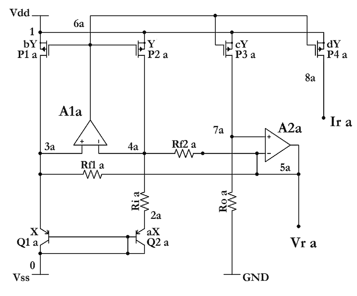
[0027]FIG. 1 is a circuit schematic showing a bandgap reference according to the Throughout this description the values of Rf1a=Rf2a=Rfa and current source values which are determined as a function of PMOS W / L scale factors may be set to a predetermined value b=c=d=1. Also note that ‘b’, ‘c’, and ‘d’ scale factors may each be in a predetermined range of 1 to 10 depending on considerations such as die size and current consumption amongst others. The current through Ria is a PTAT current where IRia has a positive TC, comprised of the difference of VEB voltages (between Q1a and Q2a) across Ria. One terminal of each of Rf1a and Rf2a is connected to the reference output Vra, with near zero TC, while each of Rf1a and Rf2a's other terminal is connected to a VEB (of Qia and Q2a) potential with a negative TC. As a result, Rfa's current IRfa will increase with temperature. Now IRia+IRfa+Ira≈0 in order to meet the requirement that sum of currents at a circuit node must be zero. Since ID of P3...

third embodiment

[0055]FIG. 3 is a circuit schematic showing a third embodiment which is an alternative bandgap reference to FIG. 2. Here, the voltage loop consisting of Ric, Q2c, A1c, and Q1c forces a difference VEB, or ΔVEB, voltage to be placed across Ric. The current ΔVEB / Ric is the IPTAT current that is mirrored via P3c onto P1c, P2c and P4c. Concurrently, VEB of Q2c feeds Rfc, which constitutes the CTAT signal. Similarly, note that Q2c is ‘a’ times the size of Q1c and P1c is ‘b’ times the size of P2c. In FIG. 3, the PTAT signal through P4c and CTAT signal through Rfc are then summed and scaled at the Vrc node, by the ratio of Rfc and ROc to generate the desired fractional VBG. With Ric connected to base of Q2c to ground, the PTAT current through Ric (e.g. in the μA level) is segregated from the quiescent current in the Q1c and Q2c BJTs (e.g. in the nA level). Running currents in Ric, Rfc, ROc at normal currents allows for small size resistors which save die costs, while concurrently running Q1...


PUM


Abstract

A family of bandgap embodiments are disclosed herein, capable of operating with very low currents and low power supply voltages, using neither any custom devices nor any special manufacturing technology, and fabricated on mainstream standard digital CMOS processes. As such, manufacturing cost can be kept low, manufacturing yields of digital CMOS system-on-a-chip (SOC) that require a reference can be kept optimal, and manufacturing risk can be minimized due to its flexibility with respect to fabrication process node-portability. Although the embodiments disclosed herein use novel techniques to achieve accurate operations with low power and low voltage, this family of bandgaps also uses parasitic bipolar junction transistors (BJT) available in low cost digital CMOS process to generate proportional and complementary to absolute temperature (PTAT and CTAT) voltages via the base-emitter voltage (VEB) of BJTs and scaling VEB differential pairs to generate the BJTs thermal voltage (VT).

Description

CROSS-REFERENCE TO RELATED PATENT APPLICATIONS[0001]The present invention claims priority from U.S. Provisional Patent Application Ser. No. 61 / 756,490, filed Jan. 25, 2013 and U.S. Provisional Patent Application Ser. No. 61 / 865,559 filed Aug. 13, 2013, both disclosures of which are herein specifically incorporated by reference in their entirety.FIELD OF THE INVENTION[0002]This invention relates to improvements in voltage regulators for integrated circuits.BACKGROUND[0003]Voltage regulators are fundamental functions in powering most analog or digital functions in electronic systems. Operating at low currents, low power supply voltages, and over extended temperatures are key objectives in portable electronics systems, including in system-on-chips (SOC), especially in medical or emerging wireless and battery-less applications such as power-on-a-chip (PoC), Internet-of-things (loT), or energy harvesting, to name a few.[0004]In light of the potentially large markets for such emerging app...

Claims


Application Information

Patent Timeline
IPC IPC(8): H02M3/158G05F3/08G05F3/16
CPCH02M3/158G05F3/08G05F3/16
Inventor FAR, ALI TASDIGHI
Owner FAR ALI TASDIGHI
Why Eureka
Try Eureka