Register file circuit design process

a circuit design and register file technology, applied in the field of register file circuit design process, can solve the problems of affecting the design flow of integrated circuits, affecting the design flow of circuits as a whole, and affecting the overall circuit complexity, so as to simplify the interface with the designer, save valuable time for the design engineer, and increase the design complexity

Inactive Publication Date: 2017-11-21
APPLE INC
View PDF10 Cites 2 Cited by
  • Summary
  • Abstract
  • Description
  • Claims
  • Application Information

AI Technical Summary

Benefits of technology

[0005]In various embodiments, a register file circuit design process is disclosed that includes a request for an automated integrated circuit design program to automatically generate at least a portion of a register file circuit design. The request may include instructions to generate several portions of the register file circuit design, including a hierarchy design, a data gating design, a read acceleration design, a write routing design, or any combination thereof. Designing some or all of the register file circuit design using the automated integrated circuit design program may save valuable time for a design engineer. Further, the automated integrated circuit design program may be able to organize the register file circuit design such that an irregularly (e.g., non-rectangular) dimensioned design may be produced in response to requested irregular dimensions.
[0006]Additionally, the automated integrated circuit design program may be able to take advantage of design layers (e.g., upper level metal layers) which may be difficult for a design engineer manually designing a register file circuit design to utilize. For example, in some cases, use of an upper level metal layer (e.g., a sixth metal layer (M6)) in a custom portion of a design may cause a design tool, in an attempt to simplify an interface with a designer, to prevent the designer from viewing details of a lower metal layer (e.g., a fifth metal layer (M5)). In some cases, the designer may view the details of the lower metal layer using a more detailed view, however, using this view may show additional circuit complexity, which may result in the designer spending additional effort to verify the custom portion of the design. Additionally, the design tool may unnecessarily prevent the design from utilizing the lower metal layer in an area of the custom portion of the design, resulting in additional design complexity. Further, because, in some cases, the design tool does not understand the functionality of a manually designed register file circuit design (and how the design may be affected by additional circuitry), the design tool may prevent higher level metal layers (e.g., layers above M6) that are associated with other portions of an integrated circuit from being routed over the manually designed register file circuit design. For example, even if the design tool recognizes that a particular area is not utilized by a manually designed register file circuit design, the design tool may prevent the particular area from being utilized by another portion of the integrated circuit in an attempt to maintain symmetry. Such an approach may result in an undesirable routing design (e.g., a routing design that is undesirably long), which may affect timing and / or area characteristics of the integrated circuit design. Accordingly, because the automated integrated circuit design program may be able to take advantage of the design layers to add additional circuitry (e.g., wires, repeaters, additional logic cells, etc.), characteristics of the integrated circuit design may be improved.
[0008]In one embodiment, the request to generate a register file design includes instructions to generate a data gating design. The data gating design may include a write pre-decode design describing a write pre-decode circuit configured to identify a plurality of entries of the register file identified by a portion of a write instruction. The data gating design may further include a gating design describing a plurality of data gating circuits configured, in response to the write pre-decode circuit not identifying a respective plurality of entries of the register file circuit, to disable at least one data input to at least one respective write selection circuit connected to the respective plurality of entries. Accordingly, in some cases, the data gating design may reduce dynamic power usage associated with unnecessarily sending the at least one data input to the at least one write selection circuit.
[0009]In one embodiment, the request to generate a register file design includes instructions to generate a read acceleration design. The read acceleration design may include a read pre-decode design describing a read pre-decode circuit configured to identify a portion of a read address, where, in response to receiving the read address, a plurality of selection circuits are configured to electrically connect a particular entry of the register file to a read port. The read acceleration design may further include a read index storage design describing a read index storage device configured to store the portion of the read address and to send the portion of the read address to a subset of the plurality of selection circuits such that the subset of the plurality of selection circuits receives the portion of the read address earlier than other selection circuits of the plurality of selection circuits. Accordingly, in some cases, data corresponding to a read may be propagated through portions of the plurality of selection circuits more quickly, which may decrease a read latency associated with the register file circuit design.
[0010]In one embodiment, the request to generate a register file design includes instructions to generate a write routing design. The write routing design may include a write port selection design describing a plurality of write port selection circuits configured, in response to a plurality of write port selection signals, to electrically connect a particular entry to a particular write port. The write routing design may further include a routing design describing encoding circuitry configured to encode a plurality of write index signals, and send the plurality of write index signals to the plurality of write selection circuits such that the plurality of write port selection signals are routed within the register file circuit design as an encoded plurality of write port selection signals, where the plurality of write selection circuits are configured, in response to the encoded plurality of write port selection signals, to electrically connect the particular entry to the particular write port. In some cases, the write routing design may reduce an area corresponding to the wires configured to carry the write port selection signals. Although the write routing design may increase a latency associated with the write port selection signals (e.g., corresponding to encoding the plurality of write index signals and to decoding or otherwise interpreting the plurality of write index signals), this tradeoff may be worthwhile due to other considerations or constraints associated with write operations (e.g., because the data written in the write operation may not be needed for several cycles).

Problems solved by technology

Integrated circuit design flow is a complex process.
Although such modifications may improve characteristics of the circuit at a local level (e.g., specific to a portion of a circuit), these modifications may negatively impact factors such as timing, area, power consumption, or routing complexity of the circuit as a whole.
Additionally, the automated integrated circuit design program may be able to take advantage of design layers (e.g., upper level metal layers) which may be difficult for a design engineer manually designing a register file circuit design to utilize.
In some cases, the designer may view the details of the lower metal layer using a more detailed view, however, using this view may show additional circuit complexity, which may result in the designer spending additional effort to verify the custom portion of the design.
Additionally, the design tool may unnecessarily prevent the design from utilizing the lower metal layer in an area of the custom portion of the design, resulting in additional design complexity.
Further, because, in some cases, the design tool does not understand the functionality of a manually designed register file circuit design (and how the design may be affected by additional circuitry), the design tool may prevent higher level metal layers (e.g., layers above M6) that are associated with other portions of an integrated circuit from being routed over the manually designed register file circuit design.
Such an approach may result in an undesirable routing design (e.g., a routing design that is undesirably long), which may affect timing and / or area characteristics of the integrated circuit design.

Method used


Image

  • Register file circuit design process
  • Register file circuit design process
  • Register file circuit design process

Examples


Embodiment Construction

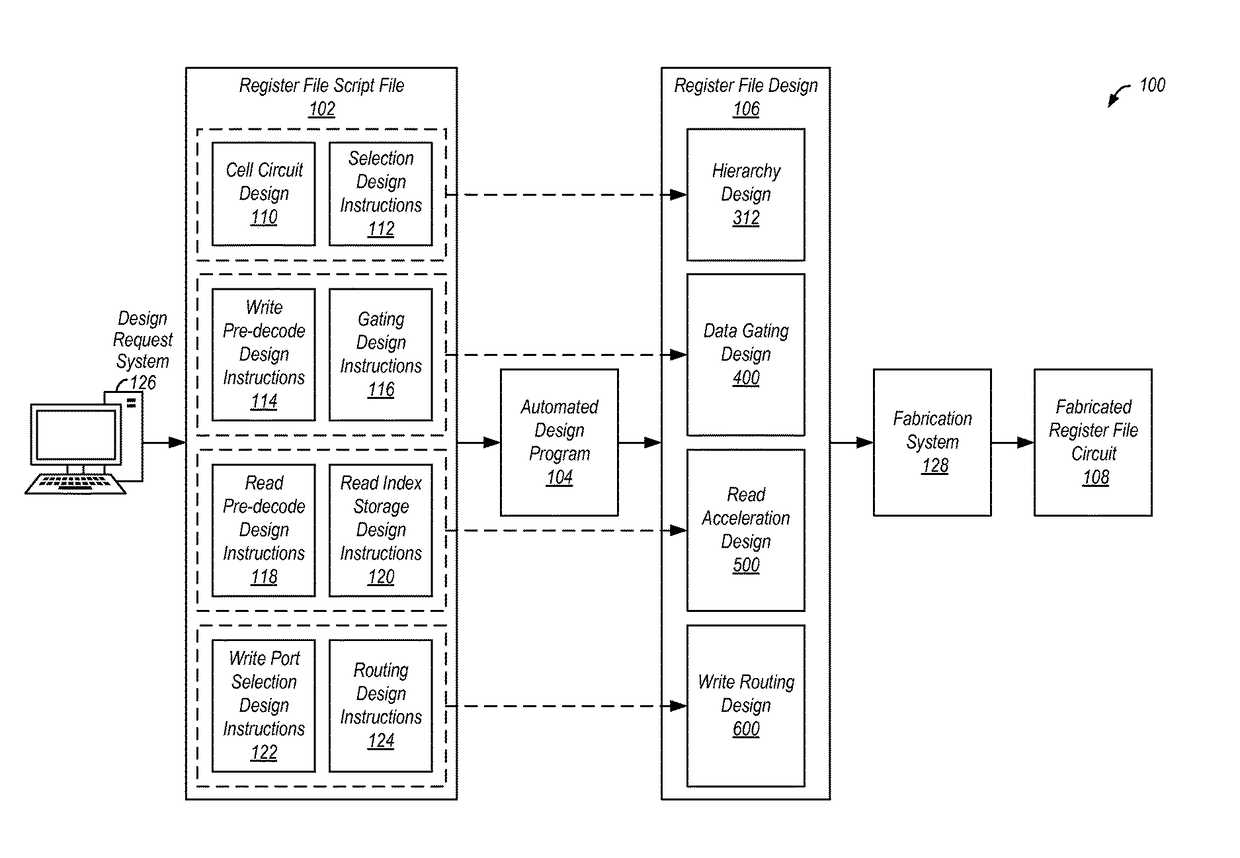
[0026]Register files are used in various functional blocks of central processing unit (CPU) design, such as being used for temporary storage of data during arithmetic, logic, data manipulation, and cryptography operations. As described above, such register files are traditionally manually designed, especially when large (e.g., 128 entries or 10,000 entries), multi-ported (e.g., 10 read ports and 4 write ports or 1000 read ports and 500 write ports), high-speed (e.g., 2 gigahertz (GHz) or 2 terahertz (THz)) designs are desired. Some or all of the processes described herein may be utilized to automatically generate such a large, multi-ported, high speed register file circuit design. This register file circuit design can be used in conjunction with a fabrication process to create a register file circuit (e.g., as part of a larger integrated circuit or as a separate circuit). Although specific numbers are provided regarding the number of entries, the number of ports, and the speed of th...


PUM


Abstract

In some embodiments, a register file circuit design process includes instructing an automated integrated circuit design program to generate a register file circuit design, including providing a cell circuit design and instructing the automated integrated circuit design program to generate a selection design, a pre-decode design, and a data gating design. The cell circuit design describes a plurality of selection circuits that have a particular arrangement. The selection design describes a plurality of replica circuits that include respective pluralities of selection circuits having the particular arrangement. The pre-decode design describes a pre-decode circuit configured to identify a plurality of entries identified by a portion of a write instruction. The data gating design describes data gating circuits configured, in response to the pre-decode circuit not identifying respective entries, to disable data inputs to respective write selection circuits connected to the respective entries.

Description

BACKGROUNDTechnical Field[0001]This disclosure relates generally to a register file circuit design process.Description of the Related Art[0002]Integrated circuit design flow is a complex process. Most often, a functional / behavioral description of the system / circuit is created with use of a register transfer language (RTL) or hardware description language (HDL) such as Verilog or VHDL (Very high speed integrated circuits Hardware Description Language). An important part of the design process is the creation of a logic implementation, and subsequently a transistor level implementation of these behavioral models. The creation of these implementations is oftentimes automated through the use of “synthesis” tools. Generally, a synthesis program is used to generate a netlist from the HDL models, making use of standard cell libraries containing a variety of circuit elements from which the integrated circuit may be constructed. Netlists usually include instances of the standard cells contain...

Claims


Application Information

Patent Timeline
Patent Type & Authority Patents(United States)
IPC IPC(8): G06F17/50
CPCG06F17/5068G06F17/505G06F30/327G06F30/39
Inventor KRISHNAMURTHY, HARSHAAGARWAL, MRIDULBALASUBRAMANIAN, SHYAM SUNDARTHOMAS, CHRISTOPHER S.GOEL, RAJATKUMAR, ROHITVELAYOUDAME, MUTHUKUMARAVELU
Owner APPLE INC
Why Eureka
Try Eureka