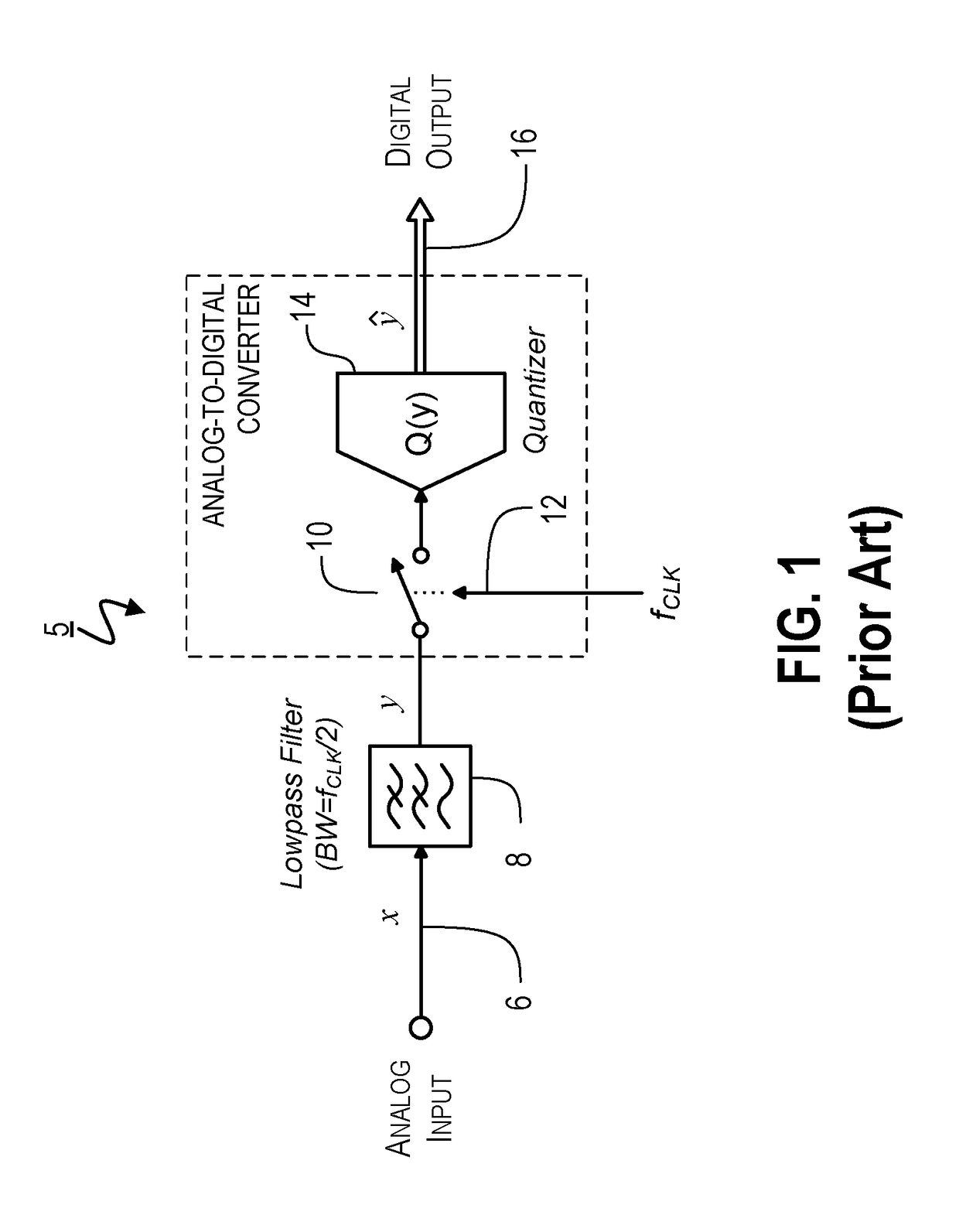
In general, the precision of an analog-to-
digital converter (ADC) is less than log2(Q) because of impairments such as sampling uncertainty, or timing
jitter, that degrade the accuracy of the sampling / quantization operation and reduce the quality of the conversion process.
Sampling
jitter / uncertainty results when the oscillator output frequency varies or drifts over time due to
resonator instabilities, and / or other circuit imperfections.
and this
noise adds directly to the converter output to degrade conversion accuracy.
Specifically, the effective resolution (i.e., ENOB) of a data converter degrades by 0.5 bits for every factor of two increase in output
noise.
The present inventor has discovered, however, that since the FTH approach employs no bandlimiting prior to the downconversion operation,
intermodulation distortion that is introduced by the input multipliers can degrade conversion accuracy.
The present inventor has discovered that a primary
disadvantage of MBΔΣ approach is increased sensitivity to timing
jitter, due to the presence of
wideband signals at the inputs of each sampling / quantization circuit (i.e., no analog bandlimiting prior to sampling and quantization).
The present inventor also has discovered that another
disadvantage of frequency
decomposition in the analog domain, as in FTH and HFB
converters, is that the practical (e.g., manufacturing) constraints associated with analog bandpass filter quality factor (i.e., quality factor Q, defined as the ratio of filter
center frequency to
filter bandwidth) limits the number of processing branches to about 25 to 30, a number which may be insufficient for realizing desired bandwidth and conversion-accuracy targets.
Although, conventionally, frequency-
interleaving converters are considered to be less sensitive to timing jitter than time-
interleaving converters, as a result of downconversion to
baseband and use of a common sampling
clock (Ding 2003), timing jitter is a problem for any converter that processes high-frequency input signals.
Conventional apparatuses for estimating instantaneous
frequency drift suffer from design limitations that make them inadequate and / or impractical for use in the correction of sampling uncertainty / jitter.
These design limitations can result from a combination of: (1) the inability to resolve small frequency fluctuations due to the relative insensitivity of conventional
delay-line discriminators (i.e., inability to resolve deviations where Δf½T, such that 2π·T·Δf is larger than π radians); and / or (3) the inability to make accurate measurements due to the susceptibility of oversampled frequency discriminators to the errors introduced by sampling
clock jitter (see Kwon, J., et al., “
Impact of Sampling
Clock Phase Noise on ΣΔ Frequency Discriminators”, IEEE Transactions on Circuits and Systems II, 2007).
The above limitations generally constrain the use of conventional discriminators to
narrowband applications, such as the
demodulation of FM signals and / or the measurement of low-frequency
phase noise, and preclude their use in jitter detection and compensation applications, which require both wide bandwidth and high
estimation sensitivity / accuracy.
Although conventional methods for extending the
usable range of
delay-line discriminators exist, these methods typically rely on the integration of multi-tiered
delay elements, and are impractical for many applications, including those targeting a
small form factor.
Adapting these conventional structures for use in Nyquist-sampled systems, or for correcting the instantaneous
frequency drift (i.e., and
resultant jitter) of a
local oscillator, however, has not been contemplated in the prior art.
However, the present inventor has discovered that at
oversampling ratios of fS / fN<8, the accuracy of conventional polynomial
estimation (interpolation) methods becomes severely degraded.
The performance of conventional analog-to-digital converters is significantly degraded by random sampling jitter, particularly at high sampling rates.
The performance of conventional time-interleaved converters is also limited by the deterministic sampling jitter, e.g., resulting from imperfections (i.e.,
skew) in the phase offsets applied to each of the subsampling clocks.
In addition, conventional methods for jitter attenuation and sample-rate conversion are only marginally suitable for use in correcting the instantaneous
frequency drift (i.e., and
resultant jitter) of a sampling
clock source.
More specifically, the present inventor has determined that conventional, PLL-based jitter attenuation methods have limited utility in converter applications due to disadvantages that include: (1) a tunable, high-precision oscillator generally cannot accommodate the wide range of conversion rates at which a converter typically needs to operate; (2) overall timing jitter is not reduced significantly because timing jitter tends to be dominated by low-frequency jitter, as illustrated in FIG. 2B (i.e., low-frequency jitter has
higher power density than high-frequency jitter); and (3) the cost and complexity may be prohibitively large because the high-precision resonators needed to implement the controlled clock source cannot be integrated onto
silicon devices using conventional methods.
In addition, conventional methods for frequency drift
estimation and sample-rate conversion are not accurate or precise enough to support
signal processing applications that require both wide bandwidth (e.g., Nyquist sampling) and high-accuracy.

