

Power converter with circuits for providing gate driving
a gate driving and power converter technology, applied in the direction of dc-dc conversion, power conversion systems, pulse techniques, etc., can solve the problems of power supply not turning, higher failure rate of smps, and more parts, and achieve the effect of superior characteristics of dc-restor
- Summary
- Abstract
- Description
- Claims
- Application Information
AI Technical Summary
Benefits of technology
Problems solved by technology
Method used
Image



Examples
embodiment # 1
Embodiment #1 Operation
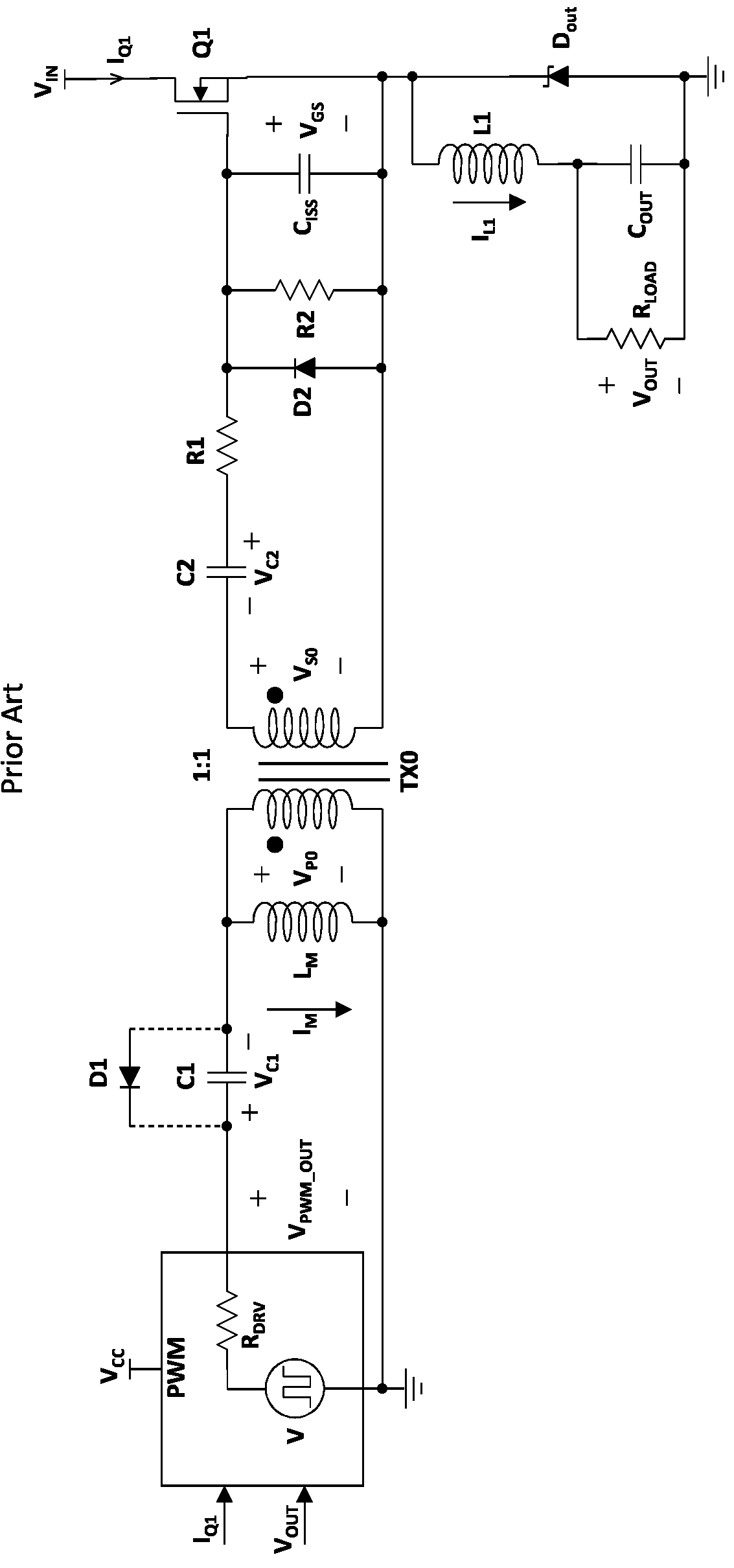
[0167]The various problems mentioned in the Background are solved with the modifications illustrated in FIG. 9 to the DC-restore circuit illustrated in FIG. 2 wherein X3 is a general four-port module containing various solutions discussed below. First, note that diode D1 across capacitor C1 is not always necessary. The major modification is that transformer TX0 has been changed to transformer TX1 having two secondary windings VS1a and VS1b with additional circuitry in X3 connected to VS1b. However, the circuit is able to retain the use of 1:1:1 windings. This means a bifilar winding could be used for VP1 and VS1a to reduce leakage inductance. This is less important for VS1b because, as disclosed below, the high resistance load dampens oscillations.
[0168]As before, VPWM_OUT (with an internal output driving resistance RDRV) is connected to the primary Vii of isolation transformer TX1 (having an internal magnetizing inductance LM) through DC blocking capacitor C1...
embodiment # 1a simulations
Embodiment #1A Simulations
[0175]FIGS. 10A-10E show the results of a simulated short circuit using the circuitry in FIG. 9A, but without diode D1 across C1. As in the Background discussion, the PWM is operating normally until t=10 psec with a duty cycle, D=0.8 which one can infer from the 8 volt value of VPWM_OUT and VC1 in FIGS. 10A and 10B, respectively. VC2 is, as in previous simulations, charging within a diode drop of VC1 during TOFF and discharging to charge Cm during TON. The voltage on the primary, VP1 in FIG. 10C, =VPWM_OUT−VC1. The scale in amps in FIG. 10E was magnified from previously so one can see the triangular charge and discharge of IL1 more readily.
[0176]At t=10 psec, a short at the output occurs suddenly and the PWM transitions quickly from a high duty cycle (0.8 in this example) to a very low duty cycle (down to 0.06) to maintain cycle-by-cycle current limiting control of the output current. The control circuit maintains a continuous output short circuit current o...
embodiment # 1b
Embodiment #1B
[0179]FIG. 9B illustrates an alternative to the circuitry in FIG. 9A, principally involving the substitution of a, preferably, small signal MOSFET for Q2 with a similar operation. The other difference is that resistor R3 is connected from the gate to source of Q2. To equilibrate VC2 to VC1 during a short-circuit TOFF, the MOSFET should be selected so that RDSON*C2OFF. With C2=33 nF and TOFF=2.6 psec, RDSONrd quadrant. If relied on instead of D2 for DC-restoration during normal steady-state operation, TOFF can be quite a bit shorter and RDSON needs to be smaller. However, smaller RDSON comes with a larger ISS> which acts as a voltage divider with C3 so power MOSFETs are not desirable. (If one is used, there is the possibility of loading down the PWM.) Alternatively, one can use the body diode of MOSFET Q2 which will conduct when RDSON*IDS>VD≈0.8 volts.
[0180]Given a ISS> of MOSFET Q2, C3 should be 3 or 4 times larger to produce VGS=7.5 to 8 volts when VS1b goes to 10 vol...
PUM
 Abstract
Description
Claims
Application Information