Vertical cavity light emitting device
a light-emitting device and vertical cavity technology, applied in the direction of semiconductor lasers, electrical devices, laser details, etc., can solve the problems of inadequately addressing the opening of the insulation layer through which a current is injected into the light-emitting layer without loss, and achieve the effect of enhancing manufacturing yield and reducing threshold curren
- Summary
- Abstract
- Description
- Claims
- Application Information
AI Technical Summary
Benefits of technology
Problems solved by technology
Method used
Image
Examples
first embodiment
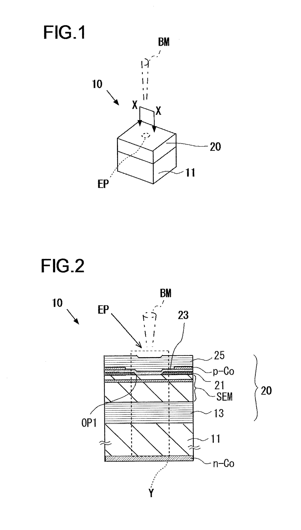
[0032]FIG. 1 is a perspective view schematically illustrating a configuration of a surface emitting laser 10 according to a first embodiment of the present invention. As illustrated in FIG. 1, the surface emitting laser 10 includes an emission port EP of a laser beam BM. The surface emitting laser 10 has a resonant portion 20 formed on a semiconductor substrate 11.
[0033]FIG. 2 is a partial cross-sectional view schematically illustrating a part of the surface emitting laser 10 along a line XX of FIG. 1.
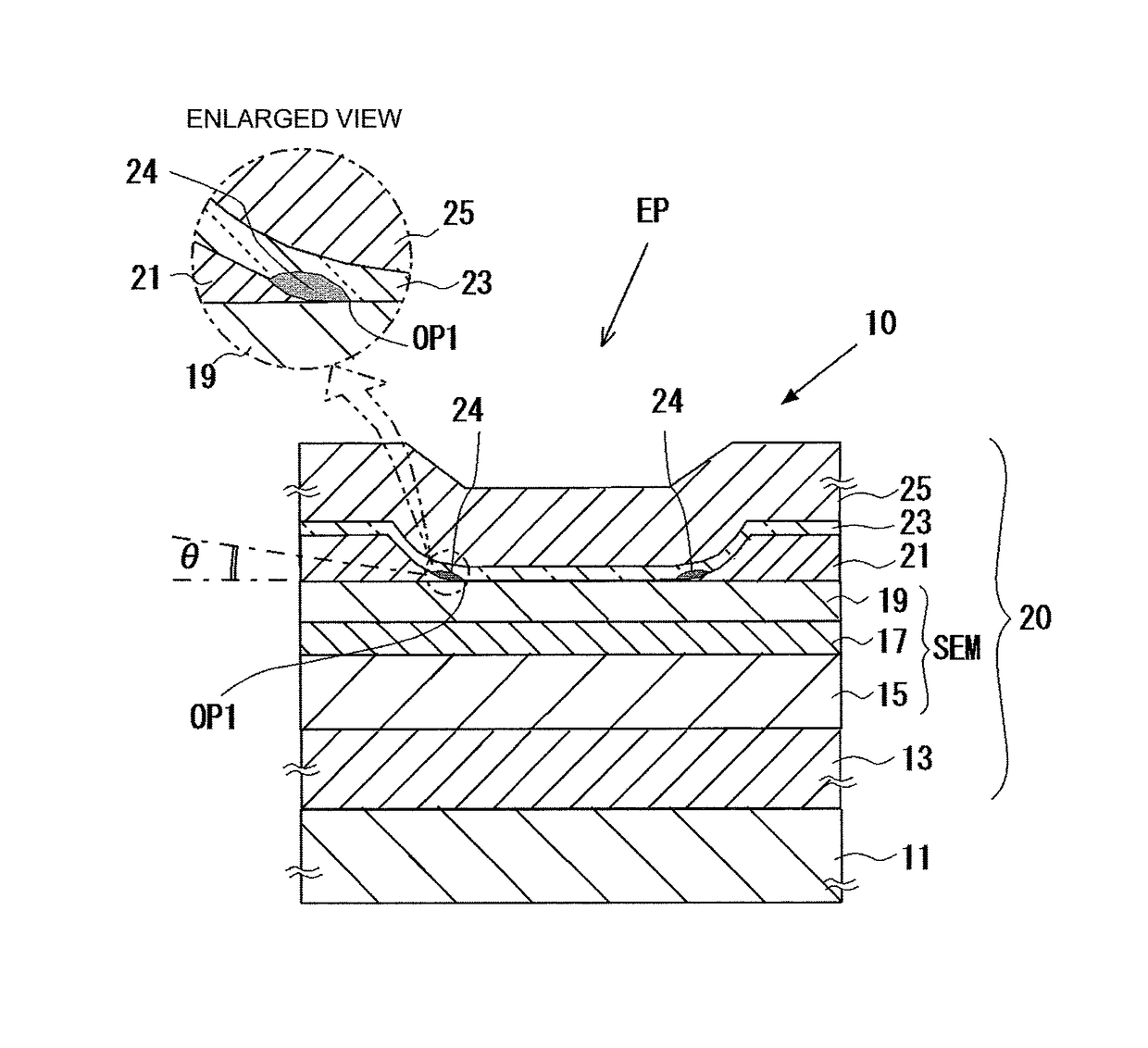
[0034]As illustrated in FIG. 2, for example, a light emitting portion of the surface emitting laser 10 includes the resonant portion 20 formed on the conductive substrate 11 comprising GaN (gallium nitride), the resonant portion 20 including a conductive first multilayer film reflector 13; a semiconductor structure layer SEM; an insulating current confinement layer; a transparent electrode 23; a p-contact layer p-Co; and a second multilayer film reflector 25. The semiconductor structur...
example
[0046]The semiconductor structure layer SEM of the surface emitting laser 10 was designed in such a manner that the emission wavelength ranged from 400 to 450 nm. The first multilayer film reflector 13, which is an electrically-conducting mirror, was designed so as to include forty laminated pairs of GaN / InAlN. The second multilayer film reflector 25, which is a dielectric mirror, was designed so as to include eight laminated pairs of Nb2O5 / SiO2.
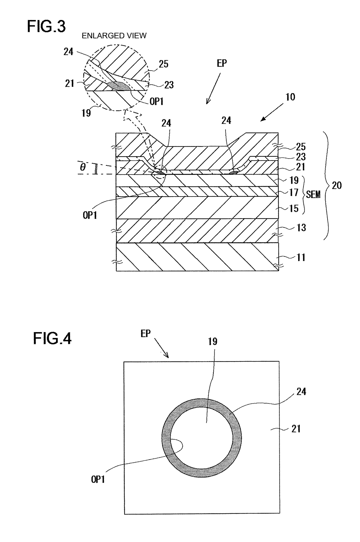
[0047]The predetermined semiconductor structure layer SEM was produced using the MOCVD method on a substrate. The SiO2 current confinement layer 21 with a predetermined thickness on the p-GaN semiconductor layer 19 was subjected to etching or liftoff method to remove SiO2 by means of chemical treatment only in the portion where the through opening OP1 (with an outer diameter of 10 μm) was to be formed.
[0048]The edge portion of the current confinement layer 21 formed along the through opening OP1 by the liftoff method specifically has the tap...
second embodiment
[0057]FIG. 9 is a perspective view illustrating an outer appearance of one surface emitting laser 10 according to a second embodiment of the present invention. FIG. 10 is a partial cross-sectional view schematically illustrating a part of the surface emitting laser 10 along a line XX of FIG. 9.
[0058]As illustrated in FIG. 10, in addition to the current confinement layer 21 and the transparent electrode 23 of the first embodiment, the surface emitting laser 10 according to the second embodiment further includes an insulation layer 21A and a driving transparent electrode 23A. Other elements of the second embodiment are substantially identical to those of the first embodiment, and a description of the configuration and operations of the elements to which the same reference numerals are assigned will be omitted here.
[0059]The surface emitting laser 10 according to this embodiment has a threshold current adjustment electrode 27 connected to the transparent electrode 23 and a pad electrod...
PUM
 Abstract
Description
Claims
Application Information


