

Semiconductor integrated logic circuit device using a pass transistor
a technology of integrated circuit and pass transistor, which is applied in the direction of logic circuits using specific components, instruments, pulse techniques, etc., can solve the problems of reducing the number of cells registered, the area of the integrated circuit and its delay time as well as power consumption becomes large, and the reduction of the number of cells is not a realistic solution. , to achieve the effect of improving the output driving capacity of cells, reducing the occupying area and reducing the area of the wiring channel
- Summary
- Abstract
- Description
- Claims
- Application Information
AI Technical Summary
Benefits of technology
Problems solved by technology
Method used
Image

Examples
Embodiment Construction
Since the basic construction and the functions of the present invention have been described above, preferred embodiments of the invention will be now explained in detail with reference to the drawings.
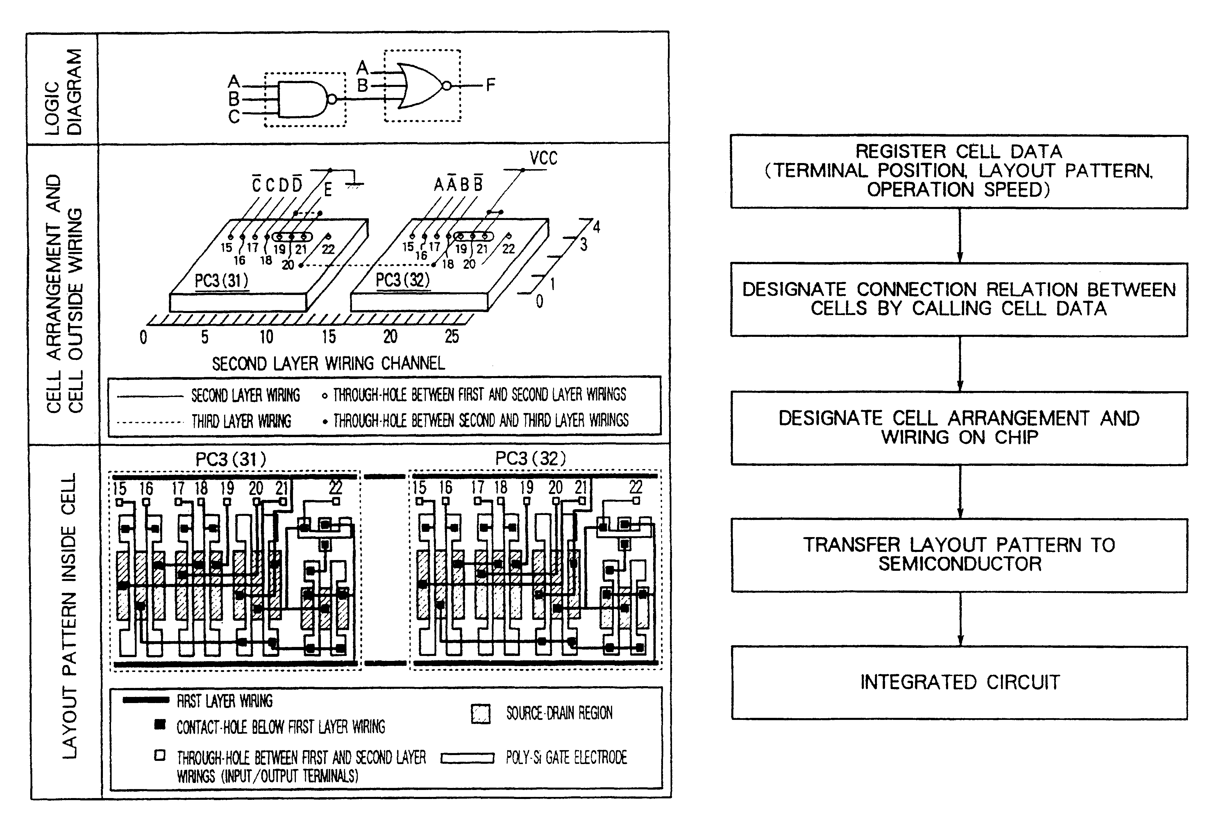
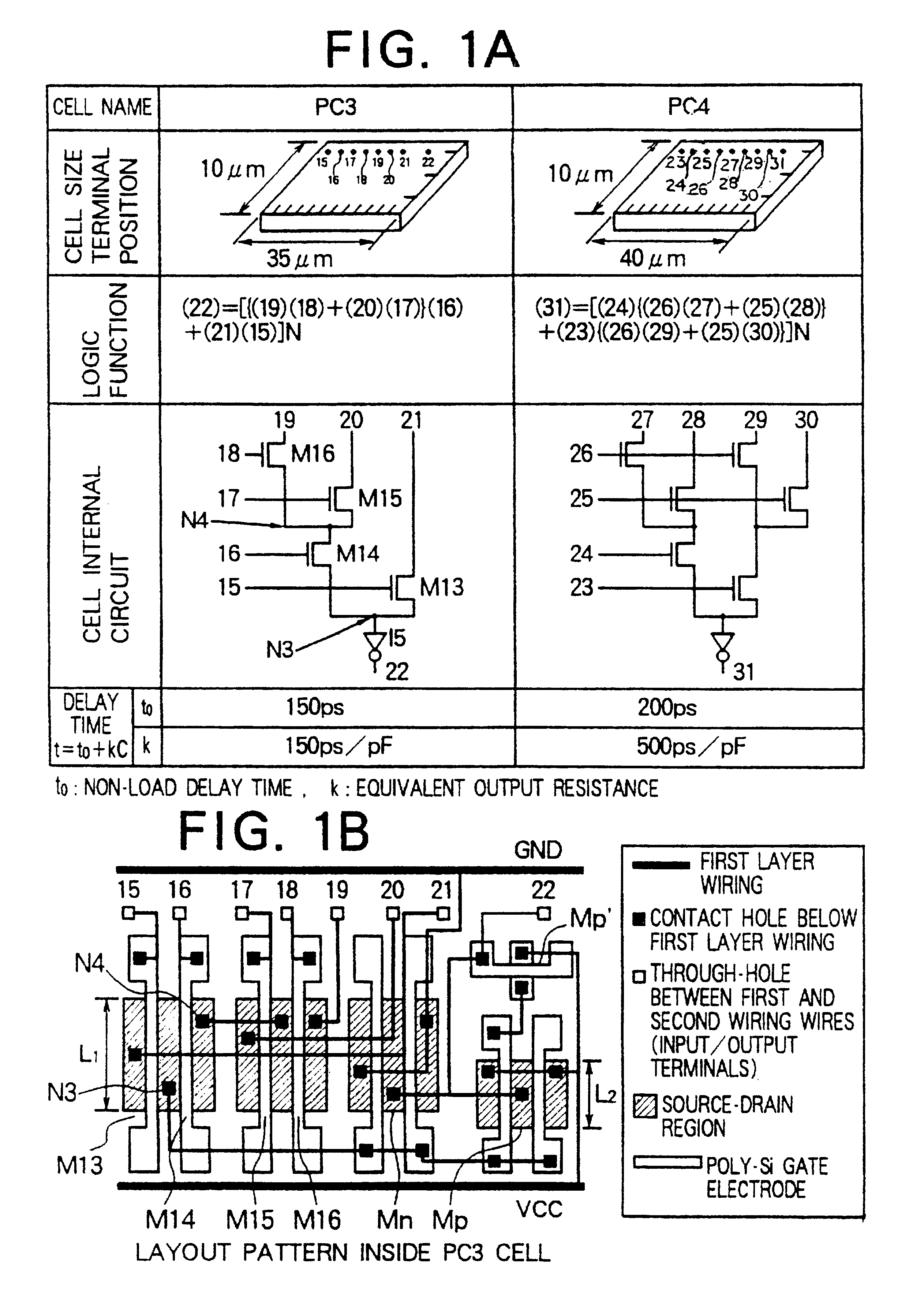
FIG. 1 shows an example of two cells registered to the cell library having the basic construction of the present invention described above. The cell size, the terminal position, logic functions, the cell internal circuit and delay time characteristics of each of the two cells PC3, PC4 are illustrated at the upper part of the drawing, and the layout pattern of the internal circuit devices of the cell PC3 is shown at the lower part.
The number of the internal circuit devices of the cell PC4 is greater by 2 than that of the cell PC3 and the number of signals of the former is greater by one than that of the latter. Accordingly, the cell PC4 can accomplish more complicated logic than the cell PC3.
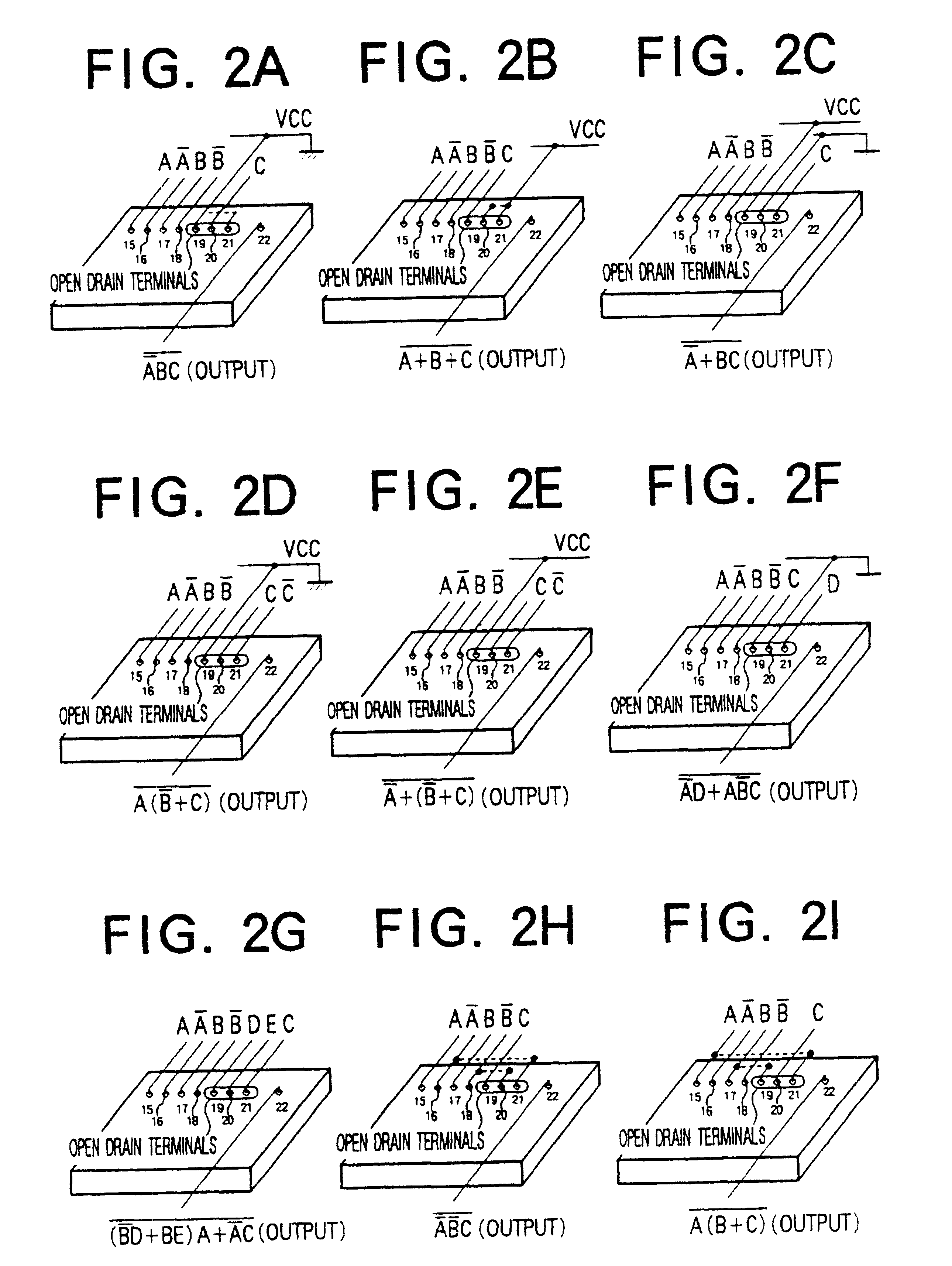
Inside the cell having a substantially square shape as represented by the layout pattern of the ...
PUM
 Abstract
Description
Claims
Application Information