
Semiconductor device and manufacturing method thereof

A manufacturing method and semiconductor technology, applied in semiconductor devices, electric solid devices, instruments, etc., can solve problems such as slow action speed, increased film resistance, difficult process combination, etc., to achieve improved reliability, miniaturization, and easy The effect formed

Inactive Publication Date: 2008-02-06
KK TOSHIBA
View PDF7 Cites 0 Cited by
  • Summary
  • Abstract
  • Description
  • Claims
  • Application Information

AI Technical Summary

Problems solved by technology

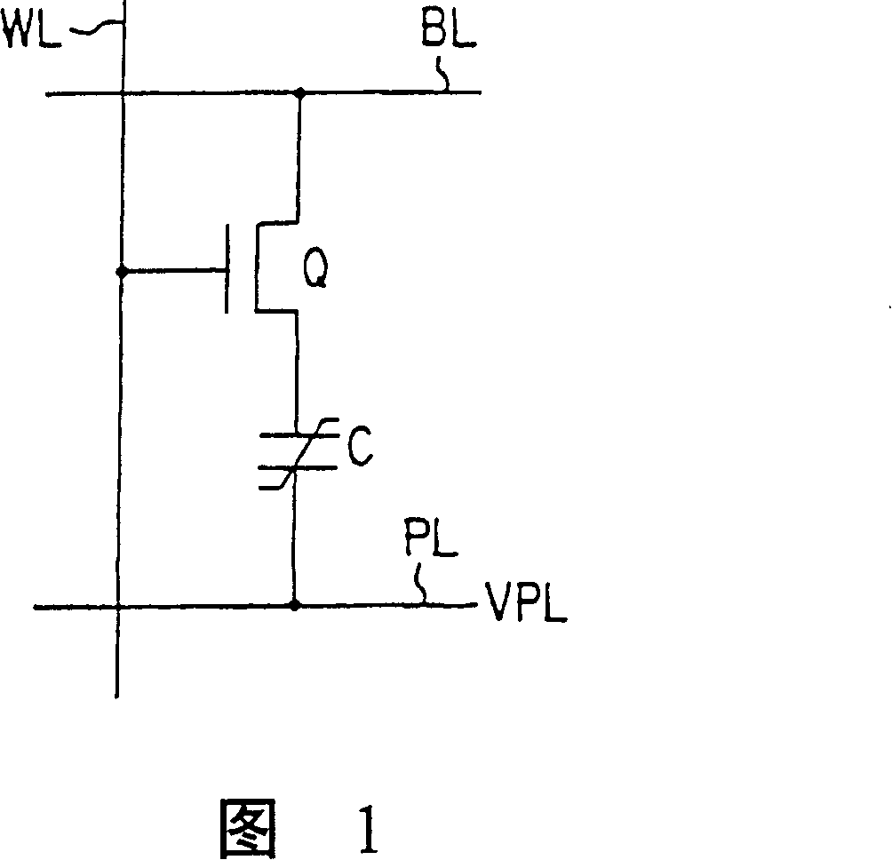
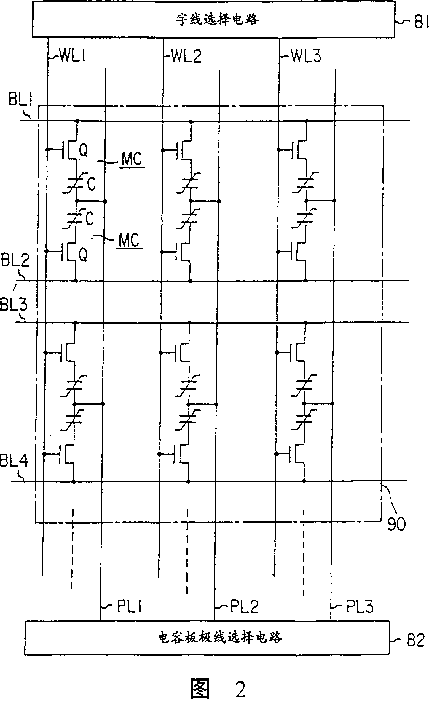
[0010] The advantage of the 1T / 1C structure is that it can achieve the same high integration as DRAM, but its disadvantage is that in order to realize a memory cell with a small characteristic dispersion, it is necessary to suppress the dispersion of the ferroelectric characteristics of the memory cell and the dispersion of deterioration, so it is difficult to improve the qualification. rate and component reliability
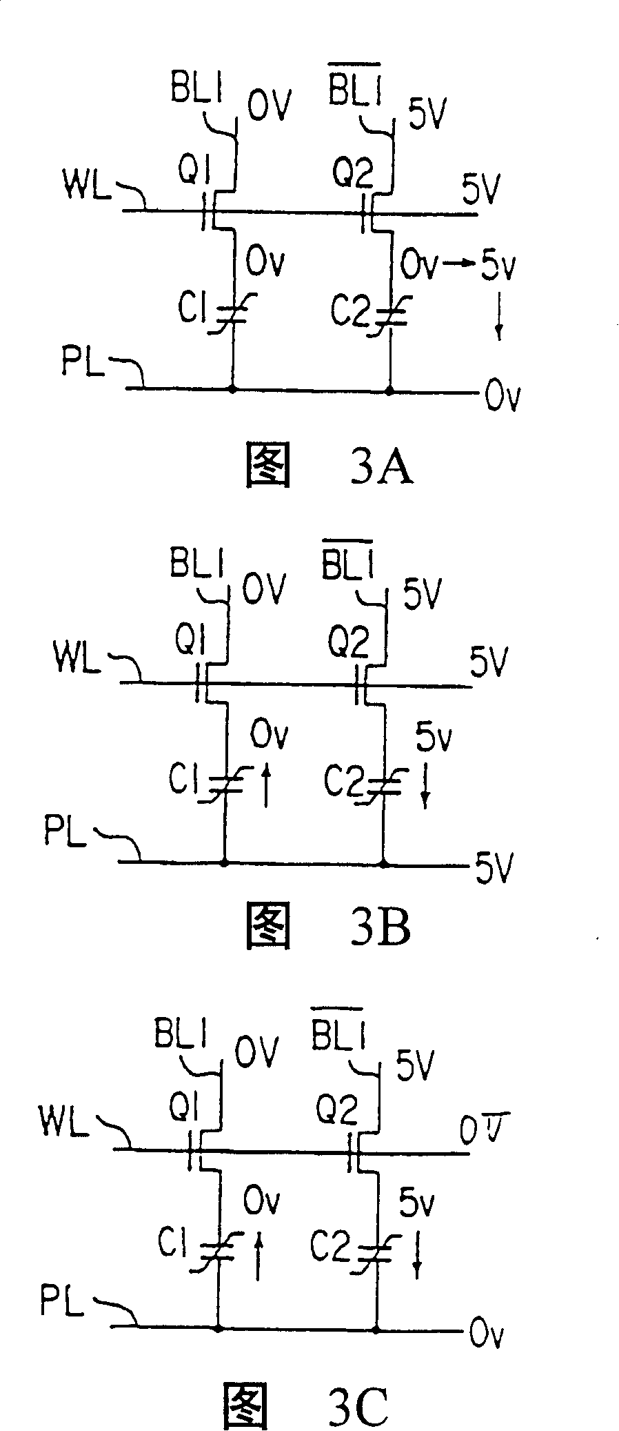
[0011] The disadvantage of the 2T / 2C structure is that it must have twice the area of ​​the 1T / 1C structure, but due to the relatively large margin of characteristics, it is easy to improve the yield and component reliability
For the same reason, once voids are formed in the electrode film and the density decreases, the problem arises that the film resistance increases and the operating speed becomes slower.
[0043] In this way, in the conventional ferroelectric memory, it is difficult to prevent the deterioration of the characteristics of the ferroelectric capacitor, and it is difficult to combine the process

Method used


Image

  • Semiconductor device and manufacturing method thereof
  • Semiconductor device and manufacturing method thereof
  • Semiconductor device and manufacturing method thereof

Examples


Embodiment 1

[0153] 6 to 8 are schematic plan views showing step by step the manufacturing steps of the ferroelectric memory cell array according to Embodiment 1 of the present invention.

[0154] FIGS. 9 to 12 schematically show a partial cross-sectional structure in the manufacturing process of the above-mentioned cell array, specifically, they are cross-sectional views including the active region and the cell capacitor along the line A-A in FIG. 8 .

[0155] First, the structure of the cell array will be described. 12 shows a cross-sectional view of the completed cell array. Compared with the previous example in which the bit line is first formed and the upper electrode connection structure is compared, the connection structure between the switching transistor and the upper electrode 19 of the ferroelectric capacitor and the structure of the upper electrode 19 are different.

[0156] In addition, in this embodiment, an FRAM will be described as an example. This FRAM has a unit cell in w...

Embodiment 2

[0214] 16 and 17 are schematic cross-sectional views of FRAM for explaining the manufacturing method of the FRAM cell and other elements mixed therewith according to the second embodiment of the present invention in order of steps. Fig. 18 is a schematic plan view of a partial cell array of the FRAM of this embodiment. The same parts as in Embodiment 1 are assigned the same reference numerals.

[0215] The manufacturing method of this embodiment is characterized in that in order to connect the second-layer wiring (bit line or other wiring) and the first-layer wiring in the two-layer wiring structure, at least Al, AlCu, AlCuSi, WSi 2 , Cu, a material (aluminum in this case) is reflowed, and the vias are buried.

[0216] In FIGS. 16 and 17 , a MOS transistor 31 for switching a memory cell and another MOS transistor 32 for a device other than the memory cell are formed on the semiconductor substrate 1 .

[0217] In the first insulating layer 10 that covers the above-mentioned t...

Embodiment 3

[0249] 19 is a schematic cross-sectional view of an FRAM showing a partial cross-sectional structure of a FRAM cell (including an SDG region and a cell capacitor) according to Embodiment 3 of the present invention.

[0250] The FRAM cell structure shown in FIG. 19 is basically the same as the aforementioned FRAM cell structure in FIG. 2 The film 51 forms a ferroelectric capacitor, and forms the second SiO2 on the ferroelectric capacitor. 2 Membrane 52 is different in this respect.

[0251] The FRAM cell manufacturing process shown in FIG. 19 is different from the aforementioned manufacturing process with reference to FIGS. 1st SiO 2 The process of film 51, (2) after forming the ferroelectric capacitor, add the second SiO2 of about 100nm by sputtering 2 The process of film 52, (3) in the 2nd SiO 2 The second interlayer insulating film 13 is deposited on the film 52, and when it selectively opens holes, the second SiO2 layer in the lower layer 2 Film 52 or 2nd SiO 2 Film 5...


PUM


Abstract

A semiconductor apparatus and manufacturing method thereof are disclosed. The semiconductor apparatus comprises the steps of forming, on a surface of a semiconductor substrate, an MOS transistor including a drain region and a source region each formed of an impurity diffusion region, forming an insulation film on the semiconductor substrate, selectively forming contact holes in the insulation film, embedding, into the contact hole, a capacitor contact plug having a lower end which is in contact with one of the drain region and the source region of the MOS transistor, forming a ferroelectric capacitor having a lower electrode, a ferroelectric film and an upper electrode, and forming an electric wire for establishing a connection between the upper electrode of the ferroelectric capacitor and an upper surface of the capacitor contact plug.

Description

technical field [0001] The invention relates to a semiconductor device with a memory cell array in which the insulating film of a capacitor for information storage adopts a composite oxide and a manufacturing method thereof, in particular to a ferrielecric random access memory (FRAM) in which a capacitor insulating film adopts a ferroelectric ) structure and method of forming the connection wiring part between the cell transistor and the cell capacitor, the bit line contact part and the memory cell, and a dynamic memory cell with a high dielectric constant dielectric (dielectric) used for the capacitor insulation film (capacitor insulation film) Structure of a memory cell of a dynamic random access memory (DRAM) of an array and a method of forming the same. Background technique [0002] In recent years, a non-volatile ferroalactic memory unit (non-volatile ferroalactic memory aell) that uses a perovskite structure or a layered perovskite structure to form a ferroelectric thi...

Claims


Application Information

Patent Timeline
Patent Type & Authority Patents(China)
IPC IPC(8): G11C11/22H01L27/10
CPCH10B12/0335H10B53/30
Inventor 望月博奥和田久美金谷宏行日高修
Owner KK TOSHIBA
Learn More