

Structure of improving gallium nitride base high electronic mobility transistor property and producing method
A high electron mobility, gallium nitride-based technology is applied in the structure and manufacturing field of improving the performance of gallium nitride-based high electron mobility transistors, and can solve the problem of reducing the channel electron concentration, reducing the channel current, and reducing the current Collapse etc.
- Summary
- Abstract
- Description
- Claims
- Application Information
AI Technical Summary
Problems solved by technology
Method used
Image

Examples
specific Embodiment
[0039] Specific examples (see Figure 3-Figure 6 ):
[0040] The structure of the invention for improving the performance of gallium nitride-based high electron mobility transistors includes:
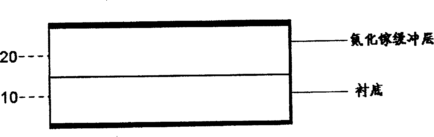
[0041] A sapphire substrate or silicon carbide substrate or silicon substrate 10;
[0042] A high-resistance semi-insulating gallium nitride buffer layer 20, the high-resistance semi-insulation gallium nitride buffer layer 20 is fabricated on the substrate 10, and the growth temperature of the fabrication is about 1000°C, the high-resistance semi-insulation gallium nitride buffer layer 20, Its growth thickness is about 2-3.5μm (see image 3 );
[0043] A high-mobility gallium nitride channel layer 30, the high-mobility gallium nitride channel layer 30 is fabricated on the high-resistance semi-insulating gallium nitride buffer layer 20, the high-mobility gallium nitride channel layer 30, its The growth thickness is about 50-100nm (see Figure 4 );
[0044] A thin layer of aluminum ...
PUM
| Property | Measurement | Unit |
|---|---|---|
| thickness | aaaaa | aaaaa |
| thickness | aaaaa | aaaaa |
| thickness | aaaaa | aaaaa |
Abstract
Description
Claims
Application Information