CMOS photoelectric integrated receiver with pre-equalizing circuit

A balanced circuit and optoelectronic integration technology, applied in the direction of electromagnetic receivers, circuits, electrical components, etc., can solve the problem of low sensitivity, achieve good reliability, reduce the number of components, and improve stability

Inactive Publication Date: 2008-08-20
TIANJIN UNIV
View PDF6 Cites 0 Cited by
  • Summary
  • Abstract
  • Description
  • Claims
  • Application Information

AI Technical Summary

Problems solved by technology

In order to overcome the shortcoming of low sensitivity of the existing photoelectric integrated receiver fully compatible with the standard CMOS process, the present invention intends to use a high-impedance amplifier with a pre-equalizing circuit to realize a photoelectric integrated receiver that can work at high speed and has high sensitivity

Method used


Image

  • CMOS photoelectric integrated receiver with pre-equalizing circuit
  • CMOS photoelectric integrated receiver with pre-equalizing circuit

Examples


Embodiment Construction

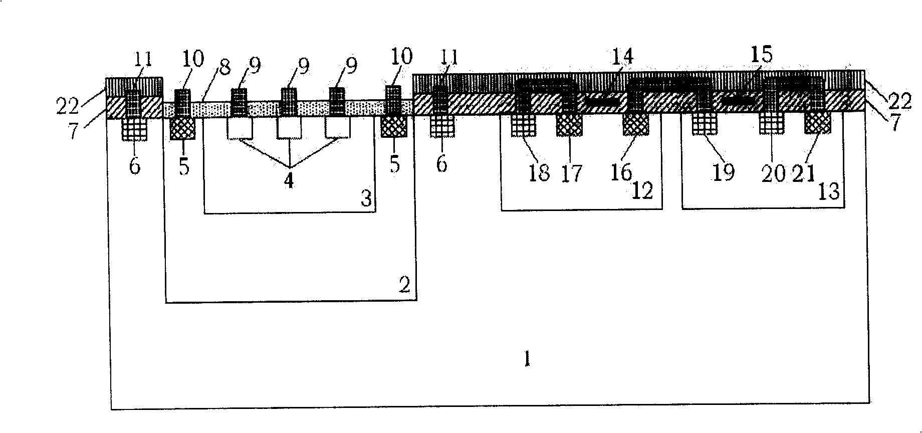
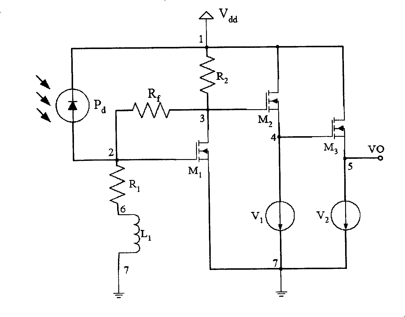
[0023] The present invention is achieved by the following methods: figure 1 It is a cross-sectional view of the structure of the photodetector compatible with the standard CMOS process, figure 2 It is a schematic diagram of the pre-equalization circuit of the silicon optoelectronic integrated receiver of the present invention. Combine below figure 1 with figure 2 To elaborate:

[0024] figure 1 The process flow of the shown photodetector is as follows: first make a deep N well 2 on the P-type semiconductor substrate 1, then make two P wells 3 and 12 in the deep N well 2 and on the P-type substrate simultaneously, deep N well 2 and P well 3 are used to make interdigital photodetectors, and P well 12 is used as an N-type MOS transistor. Then an N well 13 is fabricated on the P-type substrate, wherein a P-type MOS transistor is fabricated. Then a polysilicon layer is deposited, and gates 14 and 15 of the NMOS transistor and the PMOS transistor are fabricated by photolitho...


PUM


Abstract

A CMOS photoelectric integrated receiver with front equalizer consists of photo-electric converting component ; front equalizing circuit including buffer resistance , resonant inductance , junction capacity of photoelectric detector and input capacity of preamplifier ; and preamplifier . It is featured as connecting series circuit formed by buffer resistance and resonant inductance to place between input end and earthening end of preamplifier , forming a parallel resonant circuit by connecting said series circuit and junction capacity of silicon photoelectric detector as well as input capacity of preamplifier in parallel.

Description

technical field [0001] The invention belongs to the field of optical communication system and optical interconnection, and relates to a high-speed photoelectric integrated receiver fully compatible with standard complementary metal oxide semiconductor (CMOS) technology. Background technique [0002] An optical receiver is usually composed of a detector and a preamplifier. If both the detector and the preamplifier are fabricated on the same chip, it is called an optoelectronic integrated receiver. There have been reports of optoelectronic integrated receivers compatible with standard CMOS technology, but there are only two cases: one is that it can work at high speed but the sensitivity is too low, and the other is that it has high sensitivity and can only work at low speed, so it is compatible with CMOS technology The optoelectronic integrated receiver has not yet entered the practical stage in the field of high-speed (hundreds of megabytes to several gigabits) optical commu...

Claims


Application Information

Patent Timeline
Patent Type & Authority Patents(China)
IPC IPC(8): H01L27/14H04B10/06H04B10/60
Inventor 毛陆虹余长亮
Owner TIANJIN UNIV
Why Eureka
Try Eureka