
Producing method for complementary metal oxide semiconductor image sensor

A technology of oxide semiconductors and image sensors, which is applied in semiconductor/solid-state device manufacturing, semiconductor devices, electric solid-state devices, etc., and can solve problems such as difficulty in improving NMOS transistor characteristics and complex photodiode methods

Inactive Publication Date: 2008-11-12
CROSSTEK CAPITAL
View PDF2 Cites 0 Cited by
  • Summary
  • Abstract
  • Description
  • Claims
  • Application Information

AI Technical Summary

Problems solved by technology

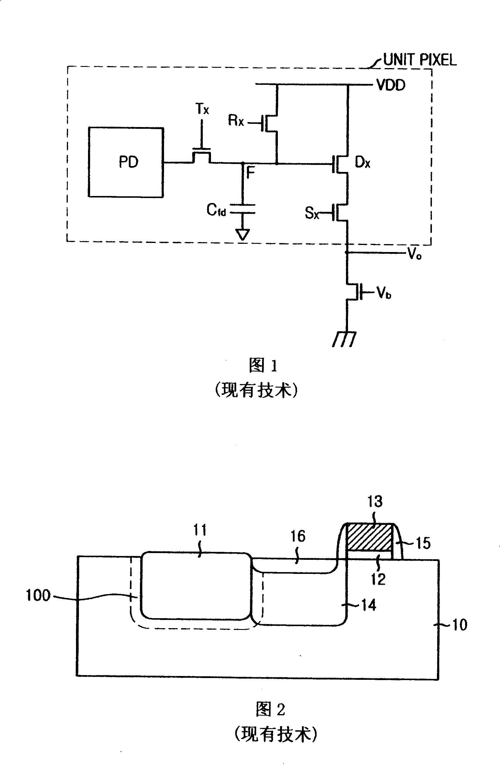
[0008] However, because the above-mentioned process of forming the photodiode implements two masking and three ion implantation processes, the conventional method of forming the photodiode is very complicated
Also, boron ions, which typically form N-channel stop regions, cause nitrogen channeling phenomena at energy levels less than about 25KeV, thereby limiting the implementation of ion implantation energies.
As a result, it is difficult to improve the characteristics of the original NMOS transistor

Method used


Image

  • Producing method for complementary metal oxide semiconductor image sensor
  • Producing method for complementary metal oxide semiconductor image sensor
  • Producing method for complementary metal oxide semiconductor image sensor

Examples


Embodiment Construction

[0015] Preferred embodiments of the present invention will be described in detail below with reference to the accompanying drawings.

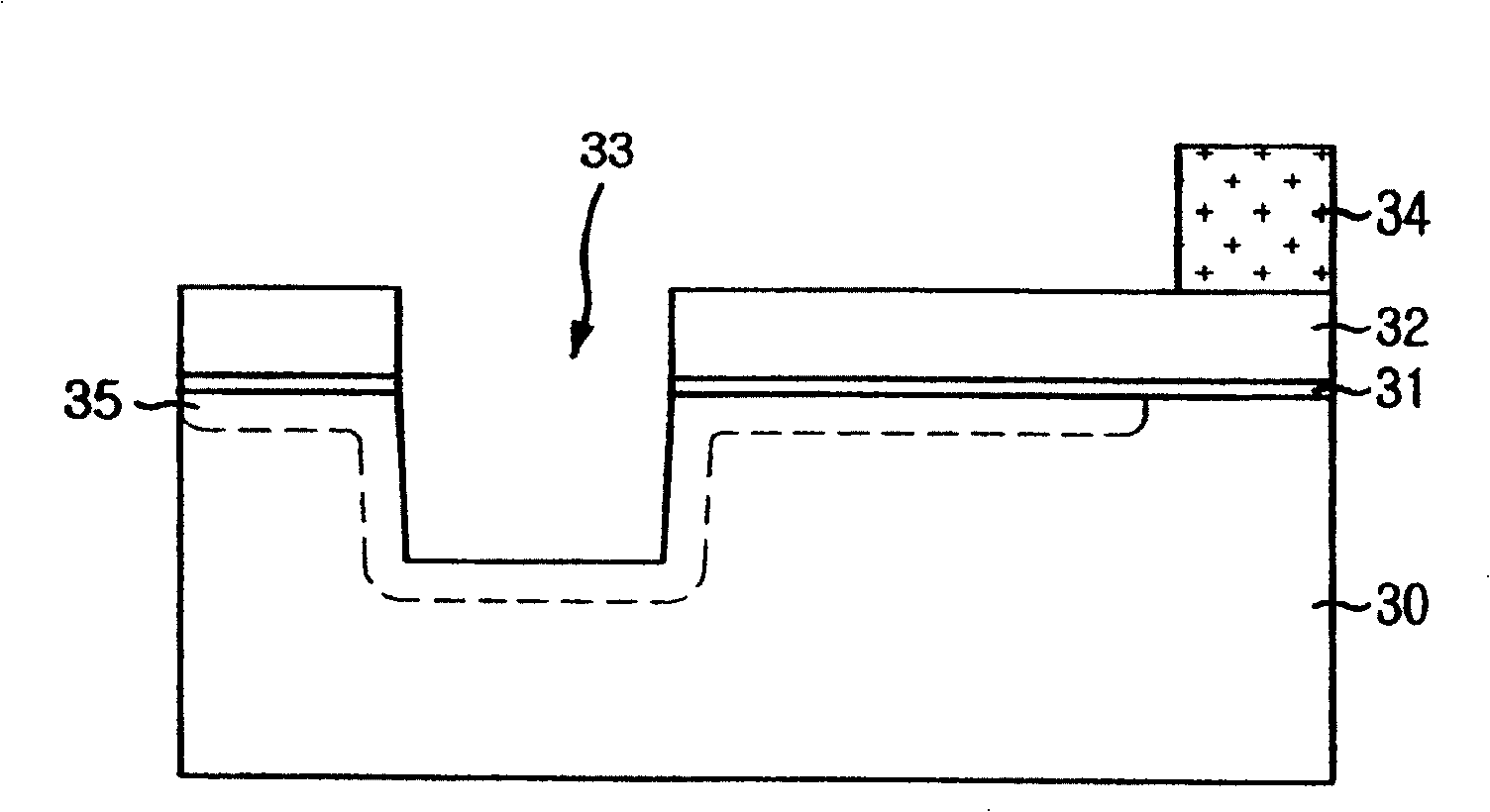
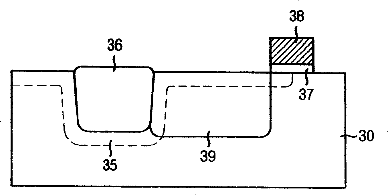
[0016] Figures 3A to 3C It is a cross-sectional view showing a method of manufacturing a CMOS image sensor according to a preferred embodiment of the present invention. Figures 3A to 3C Only a photodiode and an original transistor region are shown.

[0017] Please refer to Figure 3A , a pad oxide layer and a nitride layer are deposited on a p-type substrate 30 (providing a p-type epitaxial layer), and patterned so that a part of the p-type substrate 30 is exposed. A pad oxide layer pattern 31 and a hard mask 32 are thus formed. Here, the hard mask 32 is formed with a predetermined thickness in consideration of the channelization phenomenon occurring during a subsequent ion implantation process (for forming an N-channel stop region). Preferably, the predetermined thickness of the hard mask 32 is about to about between. Afterwards, the ...


PUM


Abstract

The present invention relates to a method for fabricating a complementary metal oxide semiconductor (CMOS) image sensor. The method includes the step of: (a) forming a substrate of a first conductive type defined with a photodiode region and a native second conductive channel transistor region; and (b) forming a first conductive type impurity region by performing an ion-implantation process for forming a second conductive type channel stop region with a first conductive impurity ion, wherein the first conductive type impurity region is extended to the native second conductive type channel transistor region.

Description

technical field [0001] The invention relates to a manufacturing method of a complementary metal oxide semiconductor (CMOS) image sensor (image sensor), especially a complementary metal oxide semiconductor image sensor capable of improving the characteristics of the original N-channel metal oxide semiconductor (NMOS) transistor Manufacturing method of the sensor. Background technique [0002] In general, a CMOS image sensor is a semiconductor device that converts an optical image into an electrical signal. The CMOS image sensor includes: a light detection unit for detecting light; and a logic circuit for processing the detected light into electrical signals, and then converting the electrical signals into corresponding data. This CMOS technology adopts a switching mode in which outputs are sequentially detected by using a plurality of MOS transistors made with the same number as pixels. [0003] The CMOS image sensor is divided into a pixel region and a peripheral region. ...

Claims


Application Information

Patent Timeline
Patent Type & Authority Patents(China)
IPC IPC(8): H01L21/76H01L21/265H01L27/146H01L21/00H01L21/82H01L27/092
CPCH01L27/14689H01L27/14609H01L27/146H01L27/092
Inventor 李源镐
Owner CROSSTEK CAPITAL
Learn More