

Chip buried-in modularize structure
A modular and chip technology, applied in electrical components, electro-solid devices, circuits, etc., can solve the problems of unformed multi-functional module structure, time-consuming production and cost, single semiconductor chip, etc., which is conducive to mass production, The effect of saving process time and shortening wiring length
- Summary
- Abstract
- Description
- Claims
- Application Information
AI Technical Summary
Problems solved by technology
Method used
Image

Examples
Embodiment 1
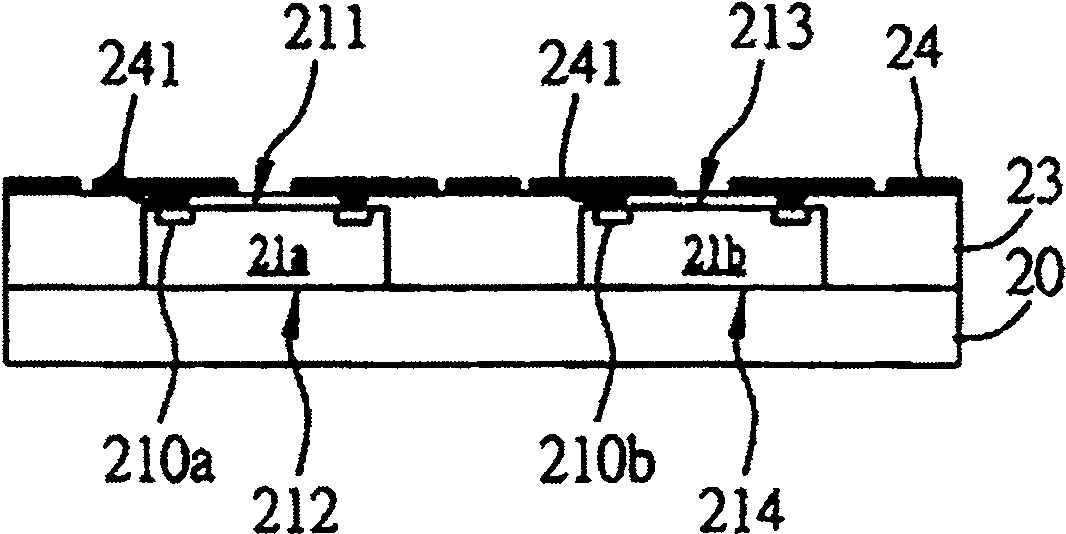
[0024] see figure 2 , which is a schematic cross-sectional view of Embodiment 1 of the chip-embedded modular structure of the present invention. As shown in the figure, the modular structure embedded in the chip includes: a first dielectric layer 20; semiconductor chips 21a, 21b, connected on the first dielectric layer 20, and formed on the semiconductor chips 21a, 21b A plurality of electrical connection pads 210a, 210b; the second dielectric layer 23, pressed or coated on the first dielectric layer 20, so that the semiconductor chips 21a, 21b are embedded in the first dielectric layer 20 and the Between the second dielectric layer 23; and the circuit structure 24, formed on the second dielectric layer 23, and the circuit structure 24 is formed in the second dielectric layer 23 through a plurality of conductive structures 241 (can be For example, conductive blind holes or bumps, etc.), are electrically connected to the electrical connection pads 210a, 210b on the semiconduc...
Embodiment 2
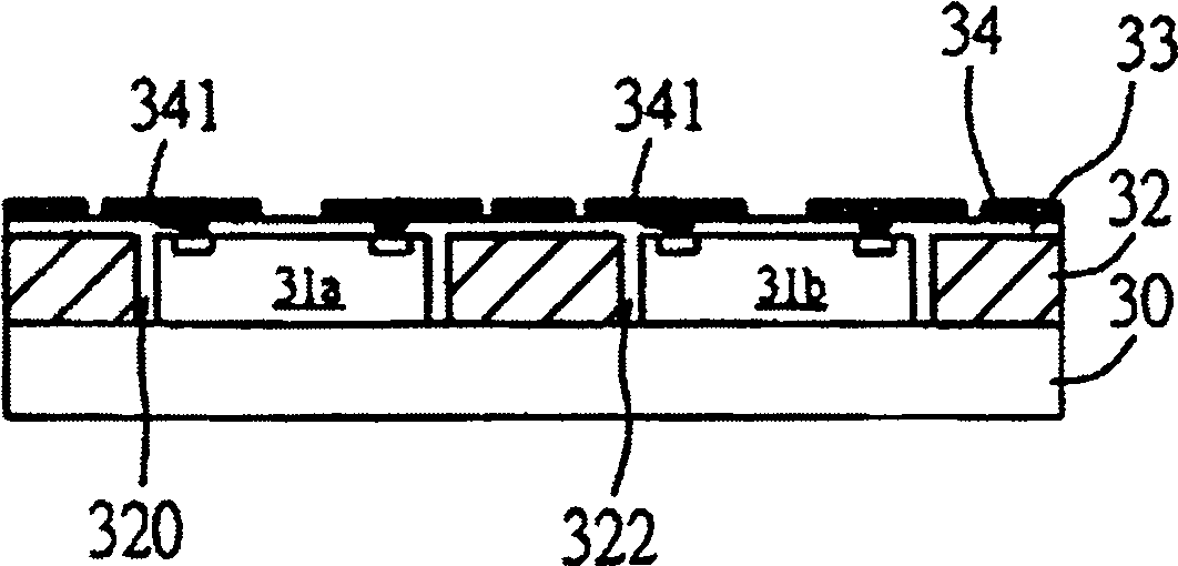
[0031] see image 3 , which is a schematic cross-sectional view of Embodiment 2 of the chip-embedded modular structure of the present invention. The structure is substantially the same as that of Embodiment 1 of the present invention, and only the differences will be described below. As shown in the figure, the main difference between Embodiment 2 and Embodiment 1 is that there is a core layer 32 between the first dielectric layer 30 and the second dielectric layer 33, and a through hole 320 is formed in the core layer 32. , 322, for semiconductor chips 31a, 31b to be accommodated in the openings 320, 322, when the second dielectric layer 33 is laminated or coated on the first dielectric layer 30 with the core layer 32 separated, the first And the second dielectric layer 30, 33 can be filled in these openings 320, 322, and these semiconductor chips 31a, 31b are embedded in their corresponding openings, and can be formed on the second dielectric layer 33 The circuit structure...
Embodiment 3
[0033] see Figure 4 , which is a schematic cross-sectional view of Embodiment 3 of the present invention. As shown in the figure, the embedded modular structure of the chip includes: a first dielectric layer 40; semiconductor chips 41a, 41b, connected to the first dielectric layer 40 and a plurality of electrical connection pads 410a, 410b are formed on the semiconductor chips 41a, 41b; the second dielectric layer 43 is pressed or coated on the first dielectric layer 40, so that the semiconductor chips 41a, 41b Buried between the first and second dielectric layers 40, 43; the wiring structure 44 is formed on the second dielectric layer 43, and the wiring structure 44 is electrically connected to the wiring structure 441 through a plurality of conductive structures electrical connection pads 410a, 410b of semiconductor chips 41a, 41b; circuit structure 45, formed on the outer surface of the first dielectric layer 40; and conductive vias 46, penetrating through the first and se...
PUM
 Abstract
Description
Claims
Application Information