
Smoothening method of rotary coating material layer and production of photoresist layer

A technology of photoresist layer and planarization method, which is applied in semiconductor/solid-state device manufacturing, photolithographic process coating equipment, electrical components, etc., can solve the problem of inability to eliminate step height difference, increase manufacturing cost, and waste process time and other problems, to avoid inaccurate focus or deviation of key dimensions

Inactive Publication Date: 2009-08-26
PROMOS TECH INC
View PDF6 Cites 0 Cited by
  • Summary
  • Abstract
  • Description
  • Claims
  • Application Information

AI Technical Summary

Problems solved by technology

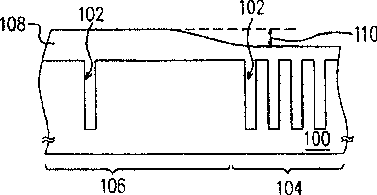
However, the above method can only gradually reduce the step height difference, but cannot completely eliminate the step height difference
Moreover, the above method requires the substrate to be repeatedly carried out between the etching machine and the photolithography machine, which not only wastes the process time, but also greatly increases the manufacturing cost
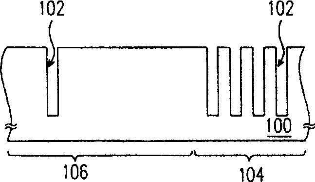
[0007] On the other hand, this phenomenon of forming step height differences is not limited to photoresist coating, and other spin-on materials such as bottom anti-reflective coating layers, spin-on glass layers, etc. can also appear in this situation, so , it is necessary to find a solution

Method used


Image

  • Smoothening method of rotary coating material layer and production of photoresist layer
  • Smoothening method of rotary coating material layer and production of photoresist layer
  • Smoothening method of rotary coating material layer and production of photoresist layer

Examples


Embodiment Construction

[0042]The present invention provides a method for planarizing a spin-on material layer, that is, a method for eliminating step height differences generated when coating spin-on material on openings with different densities in a semiconductor process. Here, the so-called spin coating materials include photoresist materials, bottom anti-reflective coating materials, spin on glass (Spin On Glass, SOG), spin on dielectric materials or any materials suitable for spin coating, etc. .

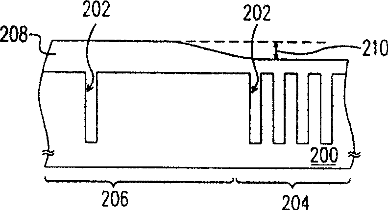
[0043] Figure 2A to Figure 2B Shown is a process cross-sectional view of a method for planarizing a spin-coated material layer according to a preferred embodiment of the present invention.

[0044] First, if Figure 2A As shown, a substrate 200 is provided, such as a silicon substrate or a semiconductor structure covered with a dielectric layer, a semiconductor material layer, or a conductive layer. There are a plurality of openings 202 on the substrate 200, and these openings 202 are, for example...


PUM


Abstract

A method of planarizing a layer of spin-coated material provides a substrate in which a plurality of openings have been formed. Then, a spin-coating material layer is formed on the substrate, and the spin-coating material layer fills up the opening. Next, a plasma etching process is performed to remove part of the spin-coated material layer until the surface of the substrate is exposed. In the plasma etching process, the substrate is cooled to maintain an etching selectivity between the substrate surface and the spin-coating material layer in the opening, so as to obtain a planarized spin-coating material layer.

Description

technical field [0001] The invention relates to a semiconductor process, in particular to a method for planarizing a spin coating material layer and a method for manufacturing a photoresist layer. Background technique [0002] In the case of higher and higher circuit integration requirements, the design of the size of the entire circuit element is also forced to advance in the direction of continuous shrinking in size. The most important process in the entire semiconductor process is the photolithography process, which is related to the structure of Metal-Oxide-Semiconductor (MOS) components, for example, the pattern of each layer of thin film (Pattern) , and the region doped with impurities (Dopants) are determined by the step of photolithography. Moreover, whether the component integration of the entire semiconductor industry can continue to be carried out with a smaller line width also depends on the development of photolithography technology. [0003] The principle of ...

Claims


Application Information

Patent Timeline
Patent Type & Authority Patents(China)
IPC IPC(8): G03F7/16H01L21/00
Inventor 卢俊男蔡念谕杨淑卿
Owner PROMOS TECH INC
Learn More