Supercharge Your Innovation With Domain-Expert AI Agents!

Method for reducing residual polymer during low-temperature nitrogen/hydrogen ashing procedure

A polymer and nitrogen technology, applied in the polymer field, can solve problems such as ineffective removal, and achieve the effect of wide adaptability and long cleaning life

Active Publication Date: 2009-08-26
SEMICON MFG INT (SHANGHAI) CORP +1
View PDF5 Cites 0 Cited by
  • Summary
  • Abstract
  • Description
  • Claims
  • Application Information

AI Technical Summary

Problems solved by technology

[0007] In order to overcome the defect that the traditional wet cleaning process cannot effectively remove the defects caused by polymers produced by DUO and other substances, and ultimately affect the performance of semiconductor devices, the present invention is proposed

Method used


Image

  • Method for reducing residual polymer during low-temperature nitrogen/hydrogen ashing procedure
  • Method for reducing residual polymer during low-temperature nitrogen/hydrogen ashing procedure
  • Method for reducing residual polymer during low-temperature nitrogen/hydrogen ashing procedure

Examples


Embodiment 1

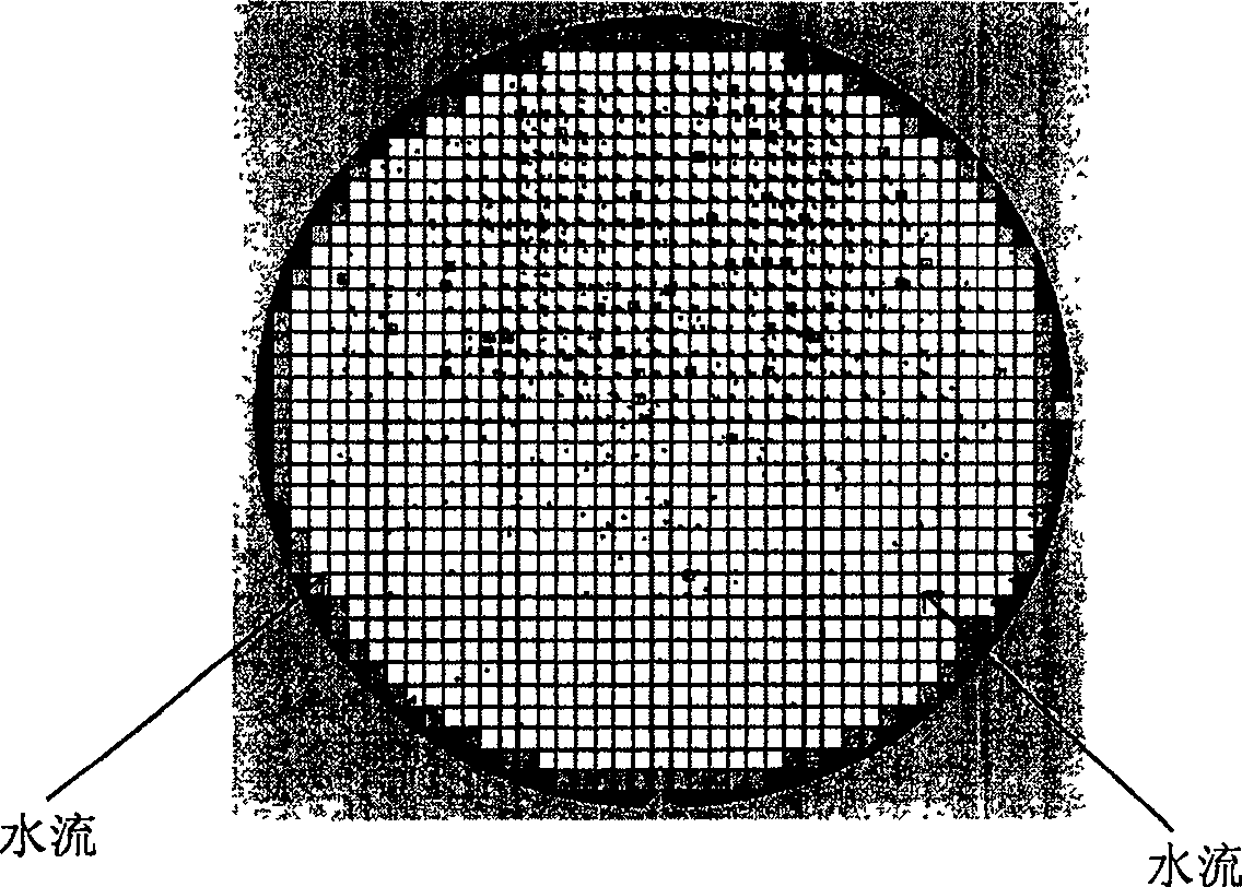
[0028] After the channel etching process is completed, a nitrogen / hydrogen ashing process is performed on the sample to be cleaned at room temperature to remove the polymer crust formed after etching. Among them, the ratio of nitrogen and hydrogen used in the ashing process, the power of the RF bias, and the duration of the process are adjusted according to the actual situation, that is, according to the degree of polymerization and hardening of the actual polymer residue, as well as the embedding method of the DUO material to adjust. The condition of ashing process in this embodiment is, N 2 / H 2 The ratio is N 2 70% and H 2 30%, RF bias 500W for 30 seconds.

[0029]Then carry out the wet cleaning process. You can use CLK888 or AP-811 produced by ATMI as a subsequent cleaning agent, or you can use DAAF produced by Daikin, or a solution containing these components. Adopt cleaning agent to be CLK888:H in the present embodiment 2 o 2 =10:1, the cleaning temperature is 50-...

Embodiment 2

[0032] In the 65nm back-end process, DUO193 is used as an anti-light reflection material. After the development and etching steps of the photolithography process, a layer of photoresist is formed on the surface of the semiconductor device, and the polymer hard skin produced by cross-linking and polymerization of DUO193 and other substances.

[0033] Nitrogen / hydrogen ashing process is performed on the sample to be cleaned at room temperature to remove the polymer crust formed after etching. Among them, the ratio of nitrogen and hydrogen used in the ashing process, the power of the RF bias, and the duration of the process are adjusted according to the actual situation, that is, according to the degree of polymerization and hardening of the actual polymer residue, as well as the embedding method of the DUO material to adjust. The condition of ashing process in this embodiment is, N 2 / H 2 The ratio is N 2 70% and H 2 30%, RF bias 500W for 30 seconds.

[0034] Then use TMAH ...


PUM

PropertyMeasurementUnit
sizeaaaaaaaaaa

Abstract

The invention provides a method for reducing polymer residues by using a low-temperature nitrogen / hydrogen ashing process. In the traditional cleaning method, the wet cleaning process is generally performed directly after the trench etching is completed. According to the method of the present invention, after the trench etching is completed , a nitrogen / hydrogen ashing process is performed at room temperature, followed by a wet cleaning process. Applying the method of the present invention can completely remove the polymer residue, thereby improving the performance of the semiconductor device; and after applying the method, the choice of the cleaning agent used for wet cleaning is more free, so that the adaptability of the cleaning process is wider; in addition, This method will not damage the low dielectric constant material and will not increase its dielectric constant.

Description

technical field [0001] The invention mainly relates to a method for removing polymers caused by photoresist and anti-light reflection materials in the back-end process of semiconductor manufacturing technology, and particularly relates to a method for reducing polymer residues by using a low-temperature nitrogen / hydrogen ashing process. Background technique [0002] In the semiconductor manufacturing process, photoresists and anti-reflective coatings such as DUO (produced by Honeywell, an inorganic anti-reflective material) are used in the photolithography process. DUO is a siloxane-based Polymers containing suitable chromophores capable of absorbing radiation at wavelengths of 248 nm and 193 nm, manufactured by Honeywell. DUO248 and DUO193 are usually used as an inorganic anti-reflective coating material in the 90nm and 65nm back-end process (BEOL, Back End of Line). Applying DUO193 is a major option for advanced semiconductor processes at or below 65nm, but DUO193 is much...

Claims


Application Information

Patent Timeline
Patent Type & Authority Patents(China)
IPC IPC(8): G03F7/42G03F7/26
Inventor 杨华郑莲晃韩秋华韩蕴高昀成
Owner SEMICON MFG INT (SHANGHAI) CORP
Features
  • R&D
  • Intellectual Property
  • Life Sciences
  • Materials
  • Tech Scout
  • Unparalleled Data Quality
  • Higher Quality Content
  • 60% Fewer Hallucinations
Learn More