Photoelectric detector for 650nm optical fiber communication and its producing method
A photodetector and optical fiber communication technology, applied in the field of photodetectors, can solve the problems of reduced minority carrier diffusion length and low short-wave photoresponsivity
- Summary
- Abstract
- Description
- Claims
- Application Information
AI Technical Summary
Problems solved by technology
Method used
Image
Examples
Embodiment Construction
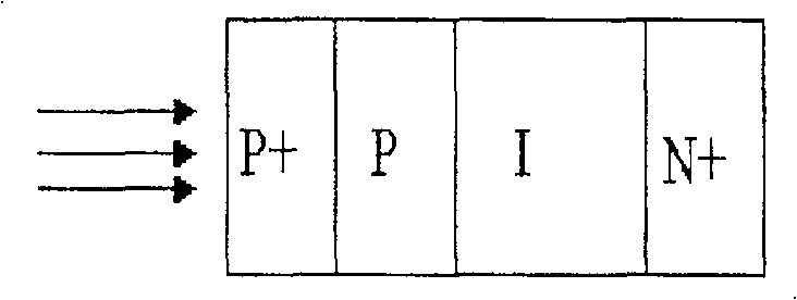
[0048] see figure 1 , the photodetector used for 650nm optical fiber communication is heavily doped P + Surface layer / P-type layer / Low-doped N - type epitaxial layer / heavily doped N + Substrate layer, namely P + / P / I(N - ) / N + Four layers of structure. After the P of the above structure + -P-I-N + Theoretical numerical simulation of the absolute spectral responsivity of silicon photodetectors with high and low emission junctions to determine the vertical structure parameters of the device.
[0049] The parameters of the epitaxial wafer of the sample are: N with a resistivity of 25.2Ω·cm - / N + Epitaxial wafer, the epitaxial layer is low-doped N - -type layer with a thickness of 36 μm. The substrate is heavily doped N + layer. The sample thickness is 580 μm. The crystal orientation is .
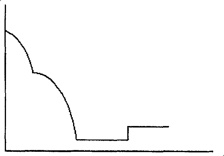
[0050] figure 2 The impurity concentration profiles of the devices are given.
[0051] P + -P-I-N + Silicon photodetectors with high and low emission junction structures ...
PUM
 Abstract
Description
Claims
Application Information


