Manufacture method of silicon substrate of insulator

A technology for silicon substrates and insulators, which is applied in semiconductor/solid-state device manufacturing, electrical components, circuits, etc., can solve the problems of difficult control of corrosion and poor uniformity of silicon on the top layer of SOI substrates, etc., to improve the corrosion selection ratio, maintain activity, The effect of improving uniformity

Active Publication Date: 2010-01-27
SHANGHAI SIMGUI TECH
View PDF2 Cites 0 Cited by
  • Summary
  • Abstract
  • Description
  • Claims
  • Application Information

AI Technical Summary

Problems solved by technology

The problem with conventional methods is that during the etching process, the etching is not easy to control, resulting in poor uniformity of silicon on the top layer of the prepared SOI substrate.

Method used


Image

  • Manufacture method of silicon substrate of insulator
  • Manufacture method of silicon substrate of insulator
  • Manufacture method of silicon substrate of insulator

Examples


Embodiment Construction

[0020] The specific implementation of the method for preparing a silicon-on-insulator substrate provided by the present invention will be described in detail below in conjunction with the accompanying drawings.

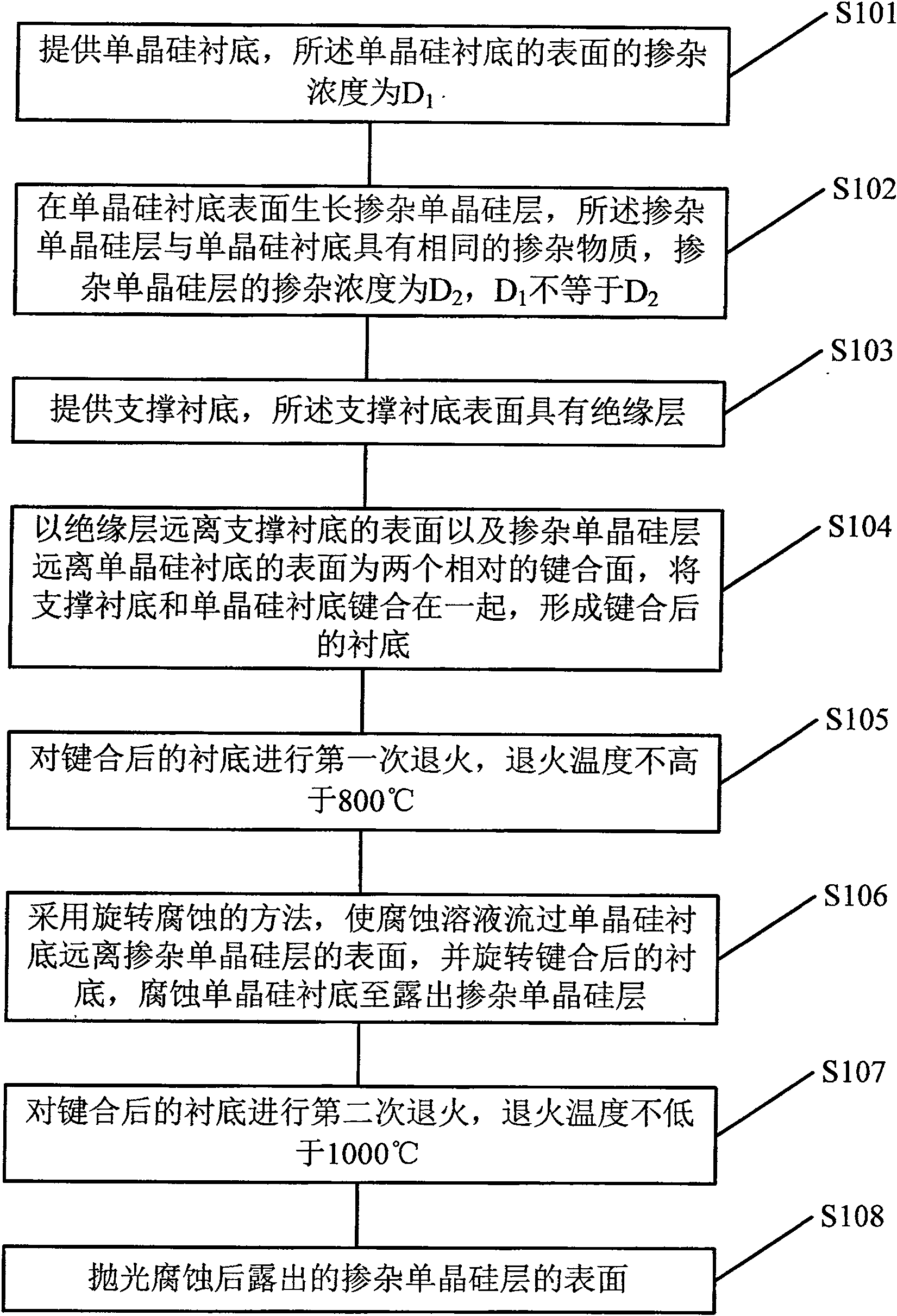
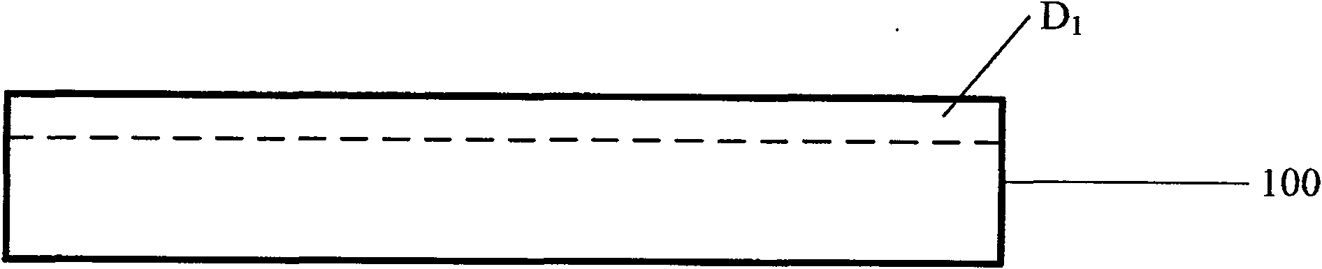
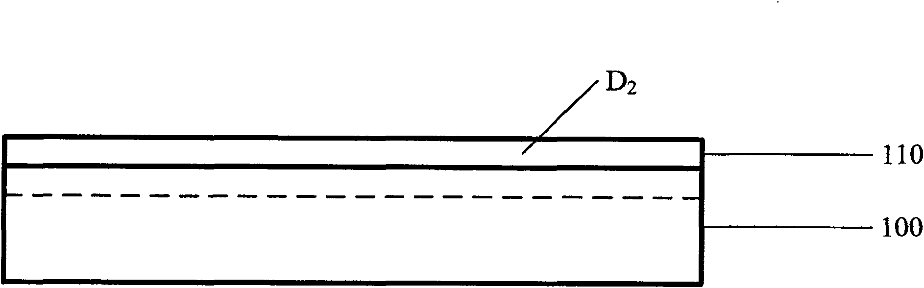
[0021] First, the first specific implementation of the method for preparing a silicon-on-insulator substrate provided by the present invention is given. figure 1 Shown is the flow chart of the implementation steps of this specific embodiment, including the following steps: Step S101, providing a single crystal silicon substrate, the doping concentration of the surface of the single crystal silicon substrate is D 1 ; Step S102, growing a doped single crystal silicon layer on the surface of the single crystal silicon substrate, the doped single crystal silicon layer has the same doping substance as the single crystal silicon substrate, and the doping concentration of the doped single crystal silicon layer for D 2 ,D 1 not equal to D 2; Step S103, providing a support ...


PUM


Abstract

A method for preparing a silicon substrate on an insulator comprises (a) providing a monocrystalline silicon substrate; (b) growing a doped monocrystalline silicon layer on the surface of the monocrystalline silicon substrate; (c) providing a support substrate; (d) bonding the support substrate and the monocrystalline silicon substrate together to form a bonded substrate; (e) annealing the bonded substrate for a first time; (f) corroding the monocrystalline silicon substrate to expose a doped monocrystalline silicon layer; (g) annealing the bonded substrate for a second time; (h) polishing the surface of the exposed doped monocrystalline silicon layer after corroding. The invention has advantages that the speed of the disengage surface doped with ions is accelerated and the activity of the corrosion solution is kept by a rotary corrosion process, thereby improving the corrosion selection ratio of the corrosion solution to the monocrystalline silicon with different doped concentrations and increasing evenness of the top layer silicon thickness of the SIO substrate. Adopting method for annealing two times can ensure the quality of the rotary corrosive interface and the fastness degree of the bonding interface at the same time.

Description

【Technical field】 [0001] The invention relates to a method for preparing integrated circuit materials, in particular to a method for preparing a silicon substrate on an insulator. 【Background technique】 [0002] Compared with bulk silicon devices, silicon-on-insulator (SOI) devices have the advantages of high speed, low driving voltage, high temperature resistance, low power consumption, and radiation resistance. rapid development. According to the thickness of the top silicon thin layer, SOI materials can be divided into two categories: thin film SOI (top silicon is usually less than 1 μm) and thick film SOI (top silicon is usually greater than 1 μm). 95% of the applications in the thin film SOI market are concentrated in 8 inches and 12 inches, and the vast majority of users are leaders in cutting-edge microelectronics technology, such as IBM, AMD, Motorola, Intel, UMC, TSMC, OKI, etc. The current suppliers are Shin-Etsu (SEH) of Japan, Soitec of France, and SUMCO of Jap...

Claims


Application Information

Patent Timeline
Patent Type & Authority Patents(China)
IPC IPC(8): H01L21/00H01L21/20H01L21/762H01L21/84
Inventor 魏星王湘张苗王曦林成鲁
Owner SHANGHAI SIMGUI TECH
Why Eureka
Try Eureka