Method for preparing polycrystal SiGe gate nano grade CMOS integrated circuit based on multi-layer assistant structure
An auxiliary structure and integrated circuit technology, which is applied in the manufacture of circuits, electrical components, semiconductors/solid-state devices, etc., can solve the problems of limited adjustment range of device threshold voltage and increased difficulty, so as to reduce process difficulty, improve manufacturing capacity, and improve performance Effect
- Summary
- Abstract
- Description
- Claims
- Application Information
AI Technical Summary
Problems solved by technology
Method used
Image

Examples
Embodiment 1
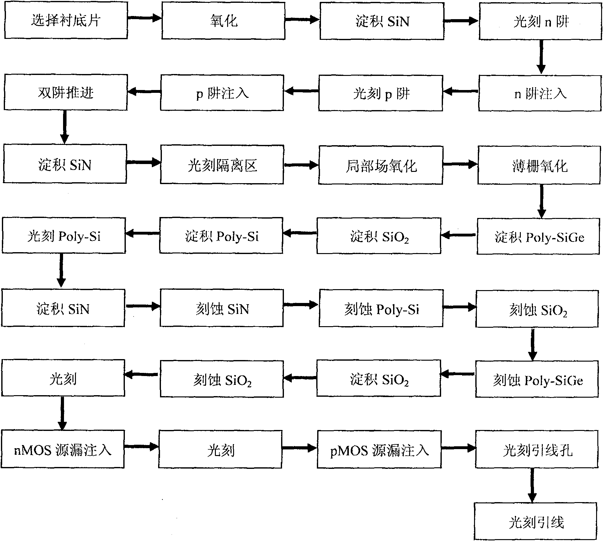
[0032] Embodiment 1: Prepare a CMOS integrated circuit with a polycrystalline SiGe gate with a 75nm conductive channel on a Si substrate. The specific steps are as follows:
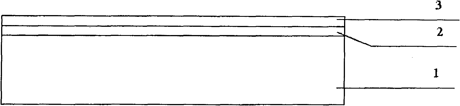
[0033] Step 1, deposit a masking layer, such as figure 2 (a) Shown.
[0034] (1a) Select the crystal orientation as , The doping concentration is 10 15 cm -3 Left and right p-type Si substrate sheet 1;
[0035] (1b) Thermally oxidize a layer of 25nm thick SiO on the substrate 2 Buffer layer 2;
[0036] (1c) In SiO 2 A 120nm thick SiN layer 3 is deposited on the buffer layer by plasma enhanced chemical vapor deposition PECVD method, which is used for the masking of the well region implantation.
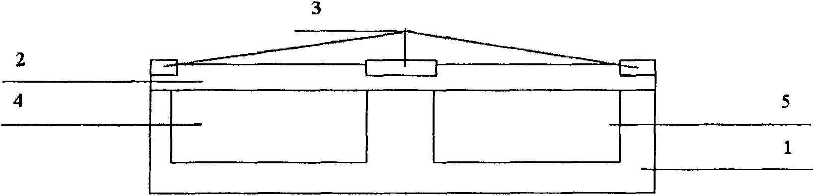
[0037] Step 2, forming a well region, such as figure 2 (b) Shown.
[0038] (2a) Photoetching the P-well region 4 and the N-well region 5 on the SiN layer 3 in the order of phases;
[0039] (2b) Boron is implanted in the P-well region to form a p-type region, and the surface of the P-well region is thermally oxidized to f...
Embodiment 2
[0068] Embodiment 2: Prepare a CMOS integrated circuit with a polycrystalline SiGe gate with a 65nm conduction channel on an SOI substrate. The specific steps are as follows:
[0069] Step 1, deposit a masking layer, such as figure 2 (a) Shown.
[0070] (1a) Select the crystal orientation as , The doping concentration is 10 15 cm -3 Left and right p-type SOI substrate sheet 1;
[0071] (1b) Thermal oxidation of a layer of 15nm thick SiO on the substrate 2 Buffer layer 2;
[0072] (1c) In SiO 2 A 100nm thick SiN layer 3 is deposited on the buffer layer by atmospheric chemical vapor deposition APCVD method, which is used for the masking of the well region implantation.
[0073] Step 2, forming a well region, such as figure 2 (b) Shown.
[0074] (2a) Photoetching the P-well region 4 and the N-well region 5 on the SiN layer 3 in the order of phases;
[0075] (2b) Boron is implanted in the P-well region to form a p-type region, and the surface of the P-well region is thermally oxidized to...
Embodiment 3
[0104] Embodiment 3: Prepare a CMOS integrated circuit with a polycrystalline SiGe gate with a 90nm conductive channel on a Si substrate. The specific steps are as follows:
[0105] Step 1, deposit a masking layer, such as figure 2 (a) Shown.
[0106] (1a) Select the crystal orientation as , The doping concentration is 10 15 cm -3 Left and right p-type Si substrate sheet 1;
[0107] (1b) Thermally oxidize a layer of 35nm thick SiO on the substrate 2 Buffer layer 2;
[0108] (1c) In SiO 2 A 130nm thick SiN layer 3 is deposited on the buffer layer by low-pressure chemical vapor deposition LPCVD method, which is used for masking the well region implantation.
[0109] Step 2, forming a well region, such as figure 2 (b) Shown.
[0110] (2a) Photoetching the P-well region 4 and the N-well region 5 on the SiN layer 3 in the order of phases;
[0111] (2b) Boron is implanted in the P-well region to form a p-type region, and the surface of the P-well region is thermally oxidized to form SiO 2 ...
PUM
 Abstract
Description
Claims
Application Information
 - R&D
- Intellectual Property
- Life Sciences
- Materials
- Tech Scout
- Unparalleled Data Quality
- Higher Quality Content
- 60% Fewer Hallucinations
Browse by: Latest US Patents, China's latest patents, Technical Efficacy Thesaurus, Application Domain, Technology Topic, Popular Technical Reports.
© 2025 PatSnap. All rights reserved.Legal|Privacy policy|Modern Slavery Act Transparency Statement|Sitemap|About US| Contact US: help@patsnap.com