Current-transfer enhanced window layer and LED with the high reflection graph shift substrate structure

A technology for light-emitting diodes and pattern transfer, which is applied in circuits, electrical components, semiconductor devices, etc., and can solve the problems of high cost, low light extraction efficiency, and a large difference between the refractive index and the air refractive index.

Inactive Publication Date: 2007-08-01
BEIJING TIMESLED TECH CO LTD
View PDF0 Cites 22 Cited by
  • Summary
  • Abstract
  • Description
  • Claims
  • Application Information

AI Technical Summary

Problems solved by technology

For example, to address the problem of absorbing substrates, someone grows a distributed Bragg (DBR) reflective layer 900 between the buffer layer and the lower confinement layer shown in Figure 1, which has a good reflection effect on photons with an incident angle close to 0 degrees , the device structure is shown in Figure 2; for the large difference between the refractive index of the LED body material and the air refractive index, the method proposed by people is to make a layer of anti-reflection film 120 on the light-emitting surface of the LED, and the external quantum efficiency of the device can be increased. About 30-40%, as shown in Figure 3; fin

Method used


Image

  • Current-transfer enhanced window layer and LED with the high reflection graph shift substrate structure
  • Current-transfer enhanced window layer and LED with the high reflection graph shift substrate structure
  • Current-transfer enhanced window layer and LED with the high reflection graph shift substrate structure

Examples


Embodiment 1

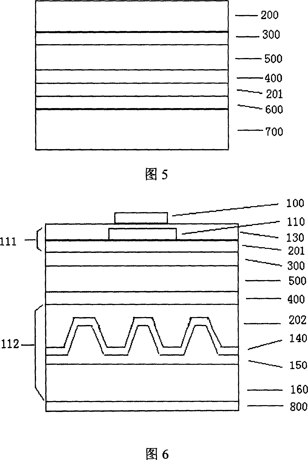
[0035] As shown in Figure 6, take AlGaInP LED as an example. The device is composed of the following parts, upper electrode 100, current blocking layer 110, conductive anti-reflection light emitting layer 130, current spreading layer 201, upper confinement layer 300, active region 500, lower confinement layer 400, patterned current spreading Layer 202, conductive highly reflective layer 140, conductive bonding layer 150, transfer substrate 160 and lower electrode 800, the preparation process and method are as follows:

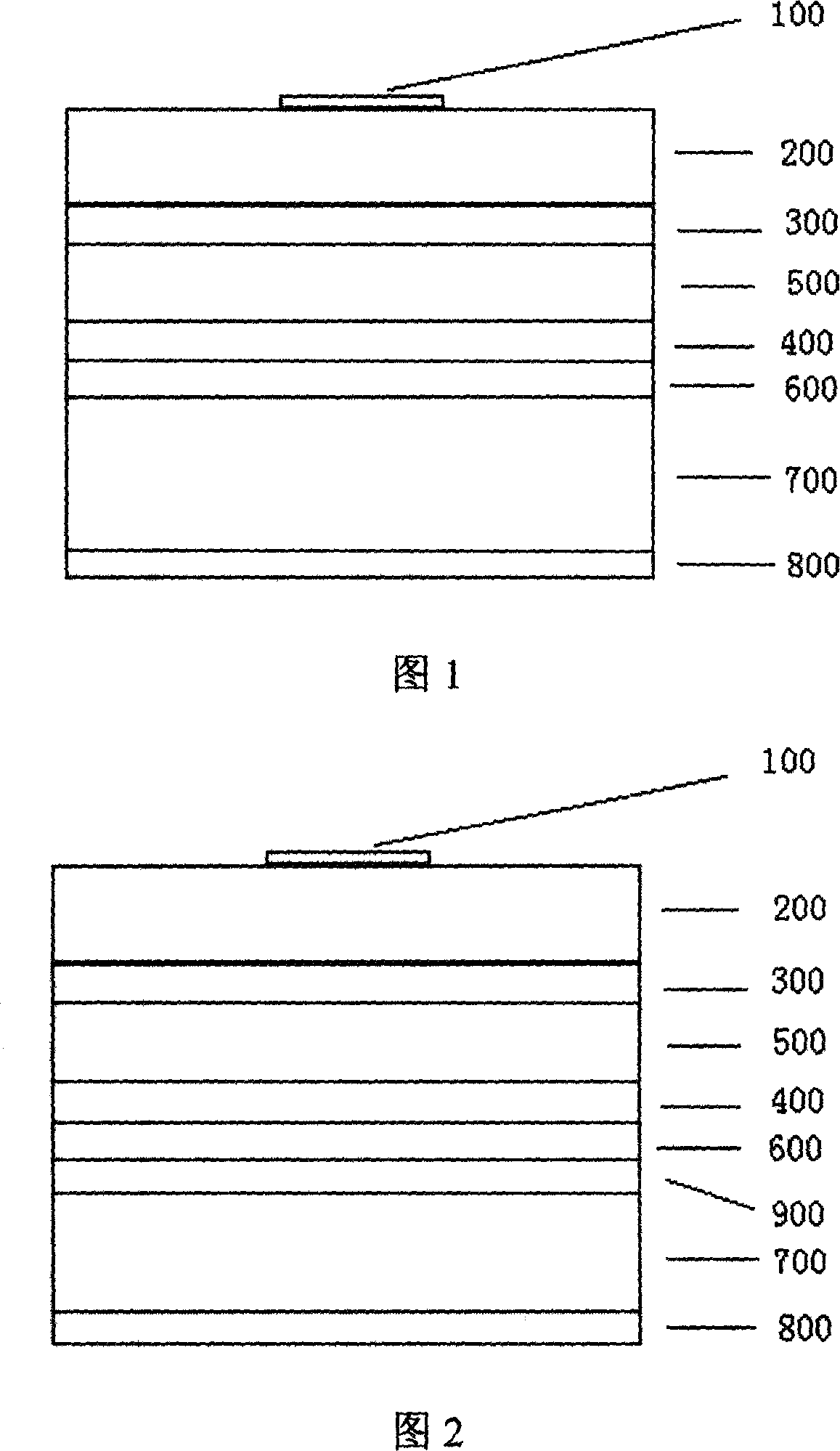
[0036] 1. Growth of the epitaxial wafer: On the substrate 700 formed of GaAs and other materials that can match AlGaInP, the buffer layer 600, the current spreading layer 201, and the lower confinement layer are epitaxially grown in sequence by the method of metal organic chemical vapor deposition (MOVCD) 400, the active region 500, the upper confinement layer 300, and the upper current spreading layer 200, so that the epitaxial wafer of the AlGaInP light-emitt...

Embodiment 2

[0045] As shown in Figure 7, take AlGaInP LED as an example. The device is composed of the following parts, upper electrode 100, current blocking layer 110, conductive anti-reflection light emitting layer 130, current spreading layer 201, upper confinement layer 300, active region 500, lower confinement layer 400, patterned current spreading Layer 202, conductive highly reflective layer 140, conductive bonding layer 150, transfer substrate 160 and lower electrode 800, the preparation process and method are as follows:

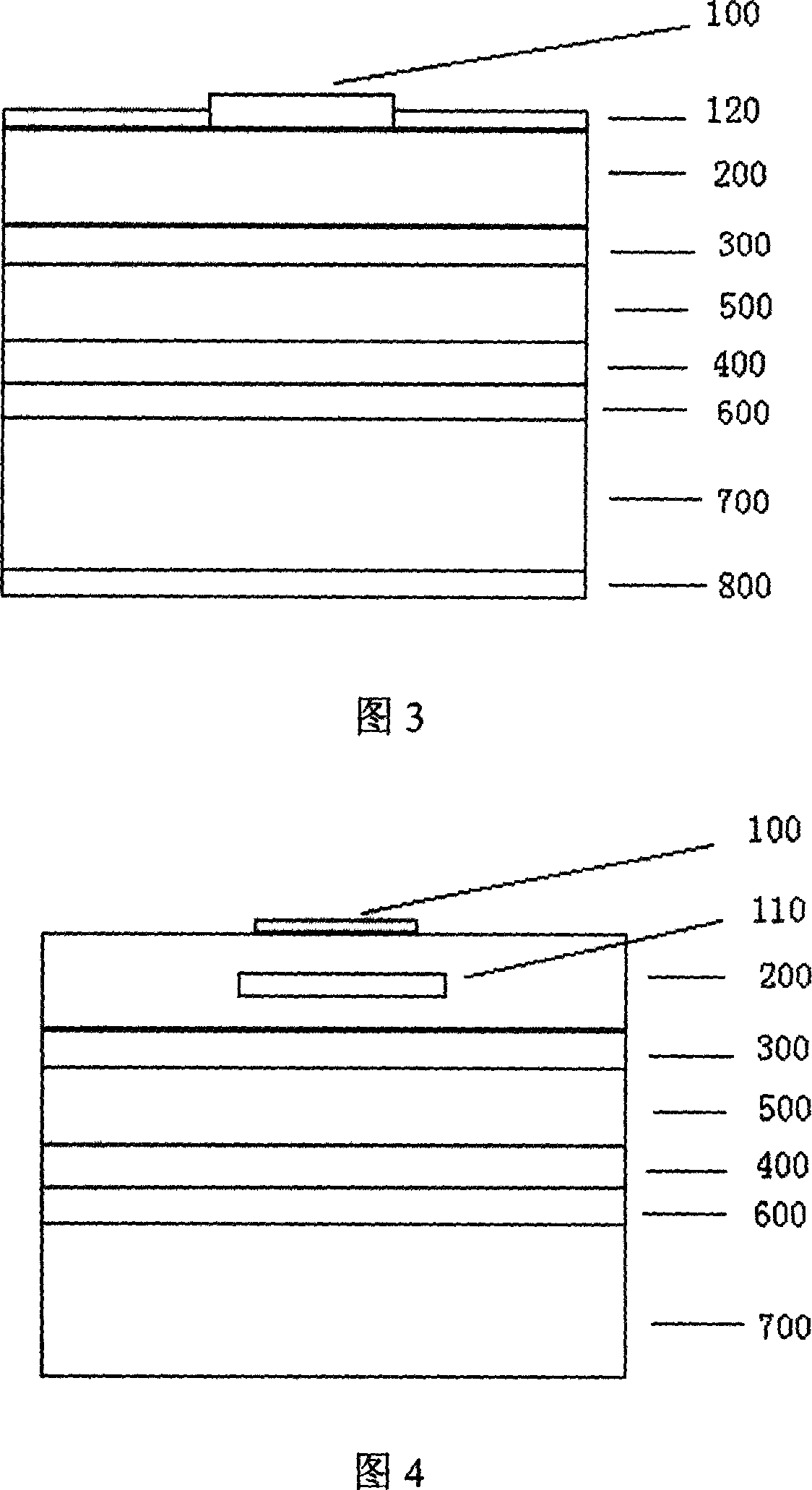
[0046] 1. Growth of epitaxial wafers: On the substrate 700 formed of GaAs and other materials that can match AlGaInP, the buffer layer 600, the current spreading layer 201, the lower confinement layer 400, the active region 500, and the upper confinement layer are sequentially grown epitaxially by using the MOVCD system. Layer 300, the upper current spreading layer 200, so just obtained the epitaxial wafer of AlGaInP light-emitting diode, as shown in Figure 5; ...

Embodiment 3

[0055] As shown in Figure 8, take AlGaInP LED as an example. The device is composed of the following parts, upper electrode 100, current blocking layer 110, conductive anti-reflection light emitting layer 130, current spreading layer 201, upper confinement layer 300, active region 500, lower confinement layer 400, patterned current spreading Layer 202, conductive highly reflective layer 140, conductive bonding layer 150, transfer substrate 160 and lower electrode 800, the preparation process and method are as follows:

[0056] 1. Growth of epitaxial wafers: On the substrate 700 formed of GaAs and other materials that can match AlGaInP, the buffer layer 600, the current spreading layer 201, the lower confinement layer 400, the active region 500, and the upper confinement layer are sequentially grown epitaxially by using the MOVCD system. Layer 300, the upper current spreading layer 200, so just obtained the epitaxial wafer of AlGaInP light-emitting diode, as shown in Figure 5; ...


PUM


Abstract

The LBD of current transmission reflection reducing window layer and high reflecting graph transfer underlay configuration belongs to field of semiconductor photoelectron technique. It includes upper electrode (100), current transmission reflection reducing window layer (111) which comprises conducting reflection reducing light layer (130), current barrier layer (110) and current expansion layer (201), upper limit layer (300), source area (500), lower limit layer (400), graphic current expansion layer (202), conducting high glisten layer (140), conducting linkage layer (150) and transfer underlay (160) or rack constructed by the upper current expansion layer (200), conducting linkage layer (150), conducting high glisten layer (140) and graphic transfer underlay (161), lower electrode (800). The invention increases the current expansion and light output, and can increase the light efficiency greatly, it can realize the high efficiency, high brightness LED lightening; the heat property and reliability are high.

Description

technical field [0001] The invention relates to a light emitting diode (light emitting diode, LED), specifically a new type of light emitting diode with an anti-reflection window layer for current transport and a high reflection pattern transfer substrate, and belongs to the technical field of semiconductor optoelectronics. Background technique [0002] At present, as a new type of light source, high-brightness visible light LEDs have a huge application market in the fields of automobile lights, outdoor displays, landscape lighting, and optical information processing. After the 1990s, the research and development of AlGaInP and GaN materials made LED develop from low brightness to high brightness and even ultra-high brightness, and the wavelength band covers all visible light regions. An important task to improve the luminous intensity of LED is to improve the luminous efficiency, including internal quantum efficiency and external quantum efficiency, although various epitaxi...

Claims


Application Information

Patent Timeline
IPC IPC(8): H01L33/00H01L33/14H01L33/20H01L33/40
CPCH01L33/405H01L33/145H01L33/20
Inventor 沈光地陈依新李建军蒋文静韩金茹
Owner BEIJING TIMESLED TECH CO LTD
Why Eureka
Try Eureka