Wafer heater assembly

A technology of heating components and heaters, applied in semiconductor/solid-state device manufacturing, electrical components, gaseous chemical plating, etc., can solve problems such as difficult control, wafer warping, metal contamination, etc., and achieve the effect of improving control

Inactive Publication Date: 2007-08-22
TOKYO ELECTRON LTD
View PDF0 Cites 25 Cited by
  • Summary
  • Abstract
  • Description
  • Claims
  • Application Information

AI Technical Summary

Problems solved by technology

In single-wafer processing, single-piece resistive heaters are used, but they are difficult to control
Issues with conventional single wafer heater systems include: potential metal contamination of components; restricted thermally isolated area (limited by heater / pedestal thermal stress cracking issues); reduced uniformity of edge heat loss effects; Mass-limited thermal response time; wafer warpage and slippage defects due to excessive thermal gradients across the wafer

Method used


Image

  • Wafer heater assembly
  • Wafer heater assembly
  • Wafer heater assembly

Examples


Embodiment Construction

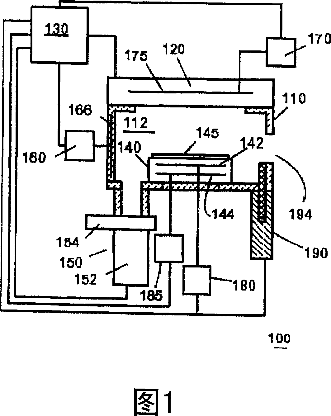
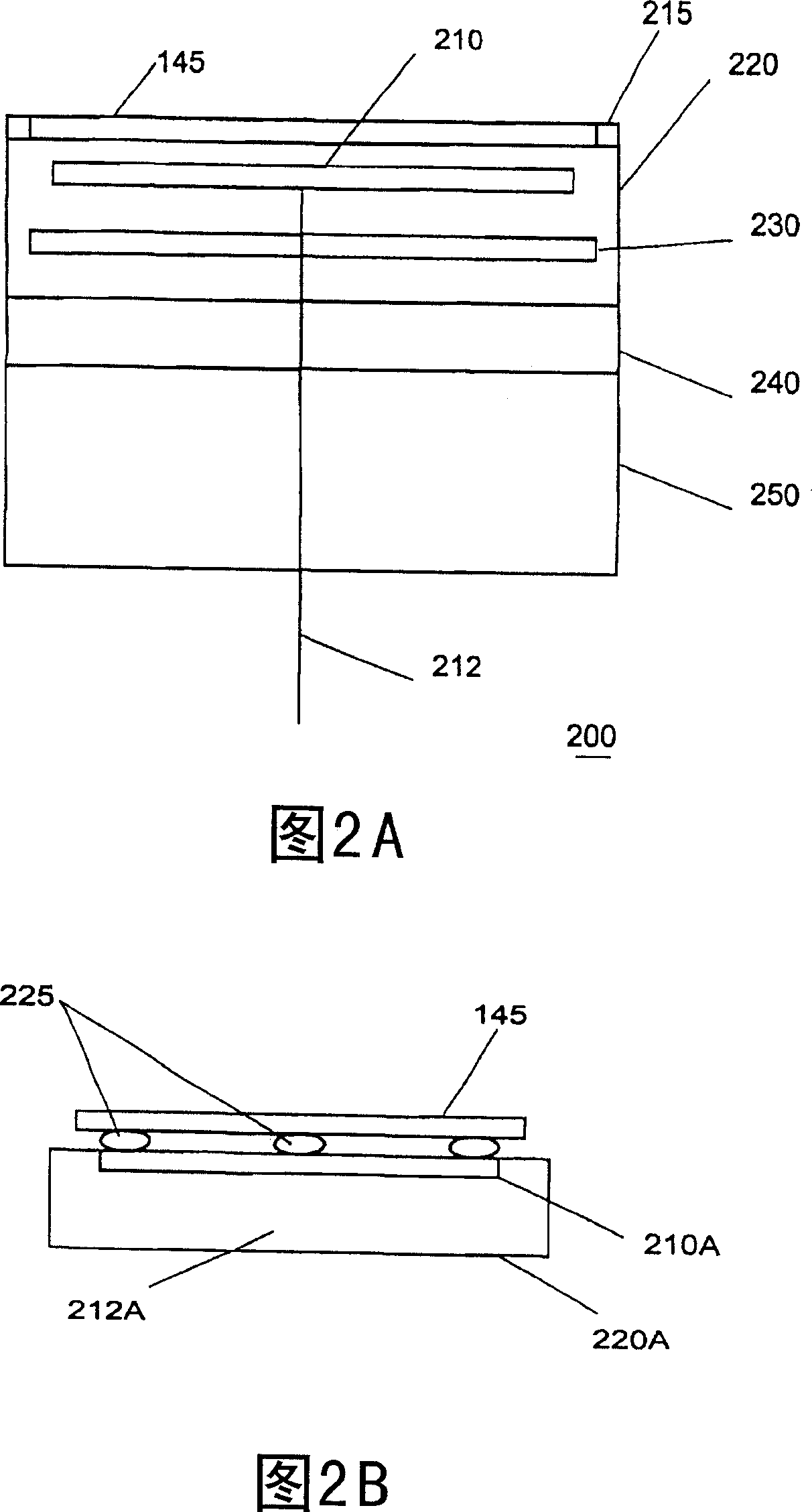
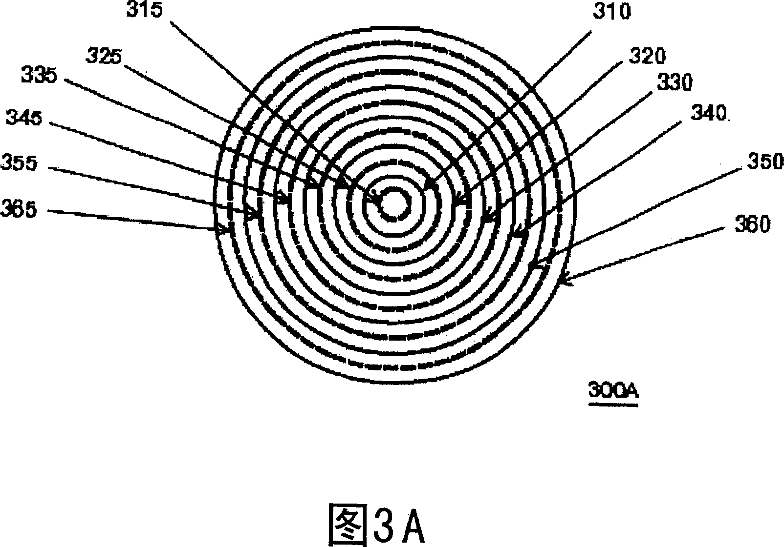
[0027] In materials processing systems, substrates and / or wafers are positioned on a holder, such as a chuck, that includes heating and / or cooling elements. In one embodiment of the present invention, an improved holder is provided that includes a unique heating element comprising high purity carbon wires embedded in quartz.

[0028] FIG. 1 shows an exemplary block diagram of a processing system according to an embodiment of the present invention. For example, processing system 100 may include an etching system such as a plasma etcher. Alternatively, processing system 100 may include a photoresist coating system, a patterning system, a development system, and / or a combination of these systems. In other embodiments, the processing system 100 may include thermal processing systems such as rapid thermal processing (RTP) systems, coating systems, chemical vapor deposition (CVD) systems, physical vapor deposition (PVD, iPVD) systems, atomic layer deposition (ALD) systems and / or c...


PUM

PropertyMeasurementUnit
diameteraaaaaaaaaa
thicknessaaaaaaaaaa
diameteraaaaaaaaaa

Abstract

A wafer heating assembly is described having a unique heater element for use in a single wafer processing systems. The heating unit includes a carbon wire element encased in a quartz sheath. The heating unit is as contamination-free as the quartz, which permits direct contact to the wafer. The mechanical flexibility of the carbon 'wire' or 'braided' structure permits a coil configuration, which permits independent heater zone control across the wafer. The multiple independent heater zones across the wafer can permit temperature gradients to adjust film growth / deposition uniformity and rapid thermal adjustments with film uniformity superior to conventional single wafer systems and with minimum to no wafer warping. The low thermal mass permits a fast thermal response that enables a pulsed or digital thermal process that results in layer-by-layer film formation for improved thin film control.

Description

technical field [0001] The present invention relates to substrate holders, and more particularly to single wafer heater assemblies having low thermal mass and fast response times in substrate holders. Background technique [0002] With the advancement of semiconductor manufacturing technology, the diameter of semiconductor wafers has been increased to provide more semiconductor circuits to meet higher requirements for higher yields and lower costs. In order to provide better yields, improved temperature control is often required. [0003] During semiconductor processing, substrate holders can be used to control the temperature of the wafer / substrate. In single wafer processing, single piece resistive heaters are used, but they are difficult to control. Issues with conventional single wafer heater systems include: potential metal contamination of components; restricted thermally isolated area (limited by heater / pedestal thermal stress cracking issues); reduced uniformity of...

Claims


Application Information

Patent Timeline
Patent Type & Authority Applications(China)
IPC IPC(8): C23C16/00C23F1/00H01L21/00
CPCH01J2237/2001H01L21/67109H01L21/683H01L21/687H01L21/00
Inventor 大卫·L·欧梅拉格利特·J·莱乌辛克斯蒂芬·H·卡巴尔安东尼·迪朴考利·瓦吉达雷蒙德·乔
Owner TOKYO ELECTRON LTD
Why Eureka
Try Eureka