Method for producing chip-bearing disc protective layer

A manufacturing method and technology for a carrier plate, which are used in semiconductor/solid-state device manufacturing, coating, and metal material coating processes, etc., can solve the problems that the protective layer is prone to dead ends, increases pollution particles, and the thickness of the protective layer is inconsistent.

Inactive Publication Date: 2007-08-29
陈国栋
View PDF0 Cites 13 Cited by
  • Summary
  • Abstract
  • Description
  • Claims
  • Application Information

AI Technical Summary

Problems solved by technology

[0007] But as we all know, the sputtering process is a high-cost technical means, which requires necessary equipment. In addition, the protective layer generated by the sputtering process on the surface of the wafer carrier disc 11 often has inconsistent thickness, especially the sputtering process. The formation of the

Method used


Image

  • Method for producing chip-bearing disc protective layer
  • Method for producing chip-bearing disc protective layer
  • Method for producing chip-bearing disc protective layer

Examples


Embodiment Construction

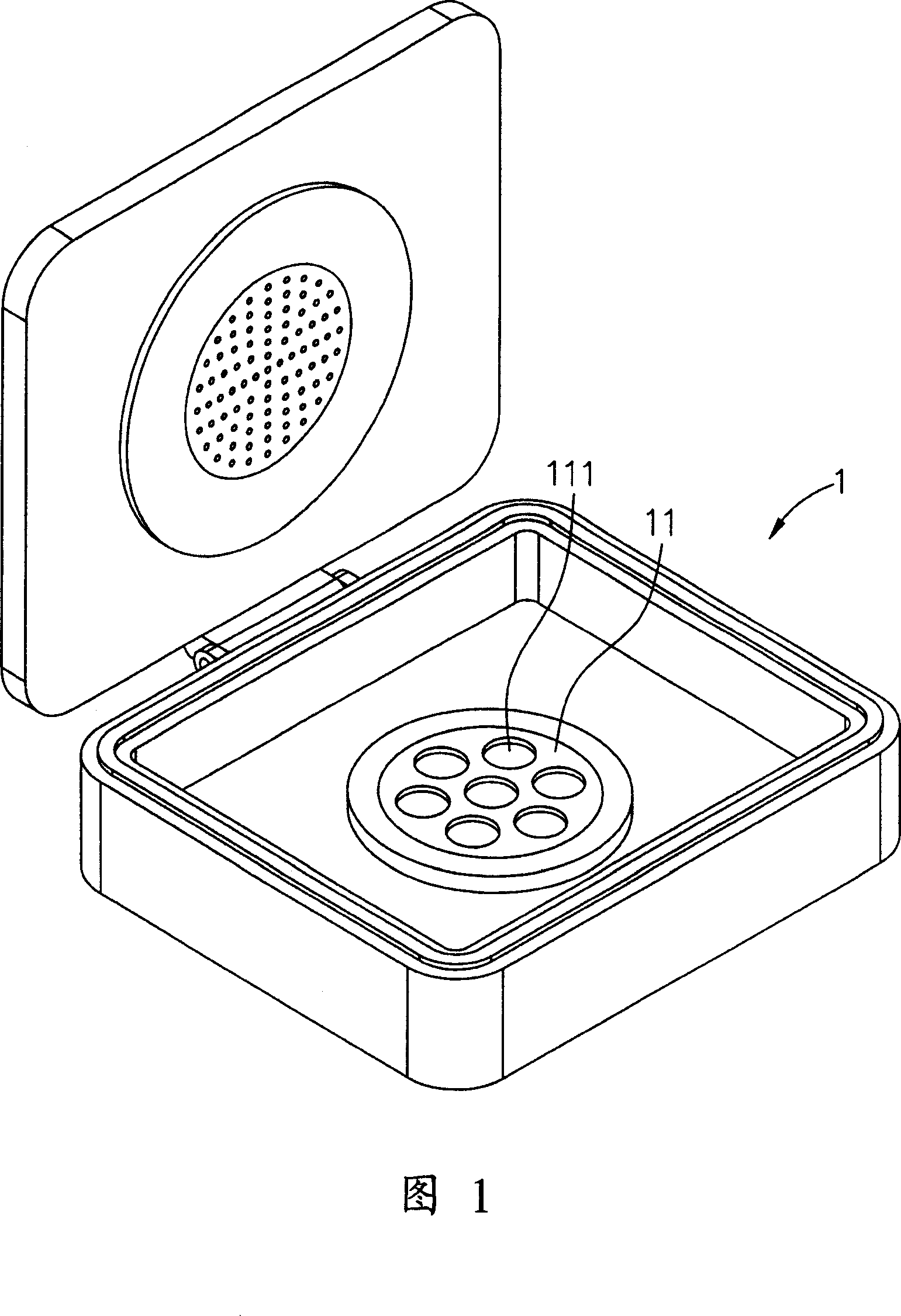
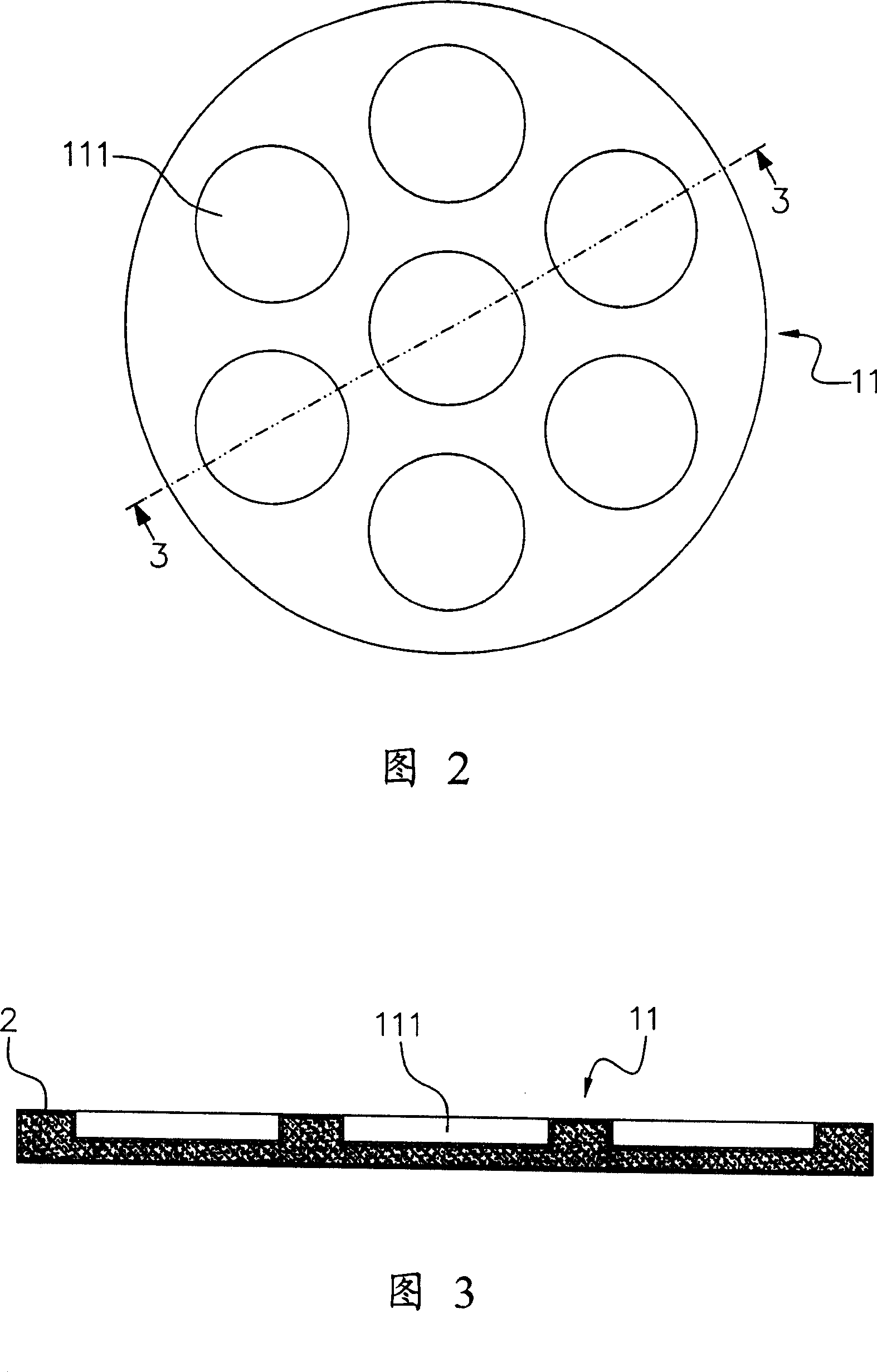
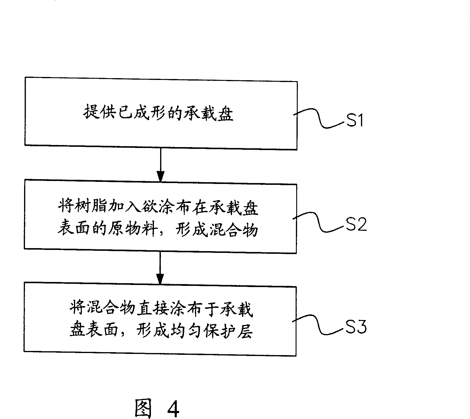
[0017] The present invention provides a method for manufacturing the protective layer of a wafer carrier. Generally speaking, the material of the wafer carrier used can be any suitable metal or non-metal, such as aluminum or graphite. In the embodiment of the present invention The wafer carrier 11 is mainly made of graphite and ceramics, as shown in FIG. 2 , a plurality of accommodating spaces 111 are provided on the carrier 11 for accommodating semi-finished wafers.

[0018] Then provide a raw material to be covered on the surface of the wafer carrier plate 11 as an anti-corrosion material, in the embodiment of the present invention, it is a silicon carbide substrate, and a resin with high temperature resistance is added to the raw material, such as glass fiber resin, silicone resin Or ceramic epoxy resin, etc., the raw material is fully mixed with the resin to form a mixture, and the resin accounts for 10% to 70% by weight of the mixture according to different types, and the ...


PUM


Abstract

The invention relates to a wafer loading disk protective layer manufacturing method. The loading wafers go along wafer manufacturing and washing process in the plant response room, improve the corrosion resistance of the loading disk, of which mainly supplies a wafer loading disk with the main material, the capacity space for containing the loading wafer installed on the front face of the loading disk, and then adding a heat resistant epoxy resin into SiC of the loading surface into a mixture, through soaking procedures to cover the mixture directly on the disk outer surface, the formation of uniform procedures baking protective layer to reduce the load disk surface spalling or deformation opportunities.

Description

technical field [0001] The invention relates to a carrying device, in particular to a carrying plate for carrying semiconductor wafers. Background technique [0002] Integrated circuits are almost ubiquitous in our daily lives. They are not only used in the computer industry that we are familiar with, but also in various consumer electronics or communication products, such as audio, television, and wireless phones. etc. In addition, the value and influence of integrated circuits in the future transportation industry (such as automobiles) and multimedia industry is also difficult to estimate, so all countries in the world are putting all their efforts into this high-tech industry. [0003] However, the manufacturing technology of integrated circuits is very complicated, requiring quite a lot of lengthy steps, and quite time-consuming, from the steps of wafer pulling, manufacturing and dicing, to the subtle VLSI manufacturing process and some common heat treatment procedures, ...

Claims


Application Information

Patent Timeline
IPC IPC(8): B05D1/00B05D7/24B05D3/02H01L21/673C23C16/54C23C16/513
Inventor 陈国栋
Owner 陈国栋
Why Eureka
Try Eureka