Process for fabricating a monolayer or multilayer metal structure in LIGA technology, and structure obtained
A structure and metal technology, which is applied in the field of new single-layer or multi-layer metal structures, can solve the problem of no forming components, and achieve the effect of good thickness control and quality improvement.
- Summary
- Abstract
- Description
- Claims
- Application Information
AI Technical Summary
Problems solved by technology
Method used
Image
Examples
Embodiment 1
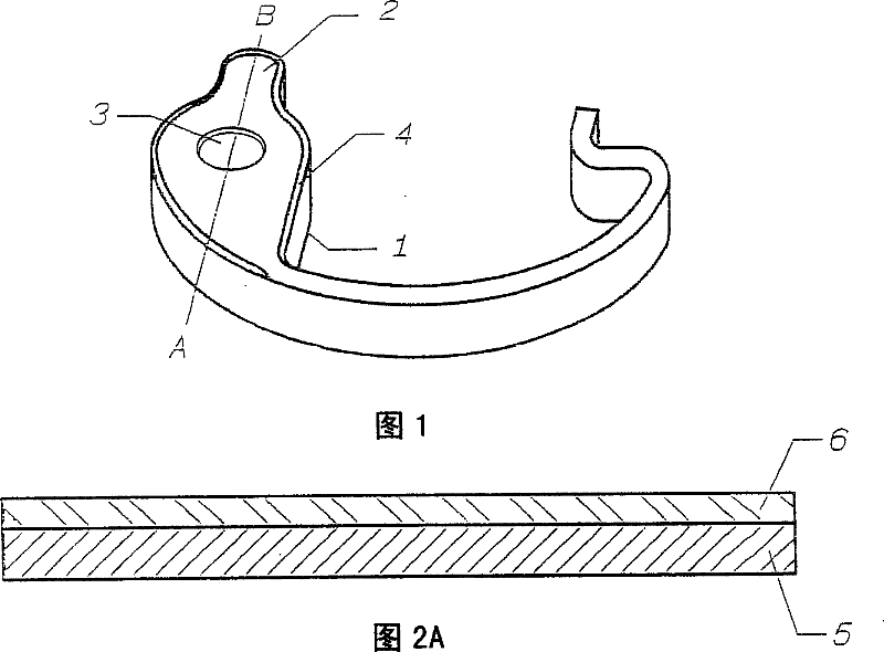
[0112] Embodiment 1: Manufacture of return spring
[0113] FIG. 1 shows a return spring with a top face 2 , a bottom face 1 , a cylindrical hole 3 and a beveled part 4 .
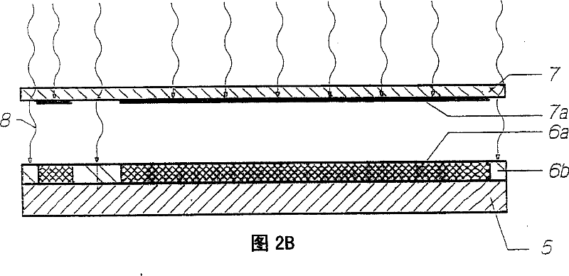
[0114] FIG. 2A shows the structure obtained after step b) of the method of claim 2 , said structure comprising a photoresist layer 6 covering the substrate 5 . This structure was obtained using the protocol described below.
[0115] A substrate 5 formed from a 1 mm thick and 150 mm diameter stainless steel plate was degreased and prepared for electroforming by degreasing with an alkaline solution, neutralizing with an acid solution to passivate its surface, and then rinsing with distilled water and dry. Next, a first layer of negative photoresist based on an octafunctional epoxy resin SU-8-2035 (Shell Chemical) with a thickness of 100 μm was deposited on the substrate 5 by spin coating, followed by heating at 65° C. minutes, and then heated at 95 °C for 20 minutes to evaporate the solvent. Next, a second...
Embodiment 2
[0122] Example 2: Manufacture of an escapement support for a watch movement
[0123] 3A and 3B show a support comprising a top surface 1 , a bottom surface 2 , a cylindrical hole 3 , a prong 4 and a notch 5 .
[0124] FIG. 4A shows the structure obtained after step b) of the method, said structure comprising a photoresist layer 7 covering the substrate 6 . This structure was obtained using the protocol described below.
[0125]A substrate 6 formed from a stainless steel plate 1 mm thick and 150 mm in diameter was degreased and prepared for electroforming by degreasing with an alkaline solution, neutralizing with an acid solution to passivate its surface, and then rinsing with distilled water , and dry. Next, a first layer of negative photoresist based on an octafunctional epoxy resin SU-8-2035 (Shell Chemical) with a thickness of 70 μm was deposited on the substrate 5 by spin coating, followed by heating at 65° C. for 3 minutes, followed by heating at 95°C for 9 minutes to ...
PUM
| Property | Measurement | Unit |
|---|---|---|
| Thickness | aaaaa | aaaaa |
| Thickness | aaaaa | aaaaa |
Abstract
Description
Claims
Application Information


