Eureka AIR delivers breakthrough ideas for toughest innovation challenges, trusted by R&D personnel around the world.

Forming method for metal silicide blocking area and method for producing semiconductor device

A technology of metal silicide and manufacturing method, which is applied in semiconductor/solid-state device manufacturing, semiconductor devices, electrical components, etc., and can solve problems such as poor adhesion of deep ultraviolet photoresist

Active Publication Date: 2007-10-10
SEMICON MFG INT (SHANGHAI) CORP +1
View PDF2 Cites 5 Cited by
  • Summary
  • Abstract
  • Description
  • Claims
  • Application Information

AI Technical Summary

Problems solved by technology

Chinese patent application document No. 98116275 discloses a layered structure for deep ultraviolet lithography and a method for forming a layered structure for photolithography, but still fails to solve the problem caused by poor adhesion of deep ultraviolet photoresist

Method used


Image

  • Forming method for metal silicide blocking area and method for producing semiconductor device
  • Forming method for metal silicide blocking area and method for producing semiconductor device
  • Forming method for metal silicide blocking area and method for producing semiconductor device

Examples


Embodiment Construction

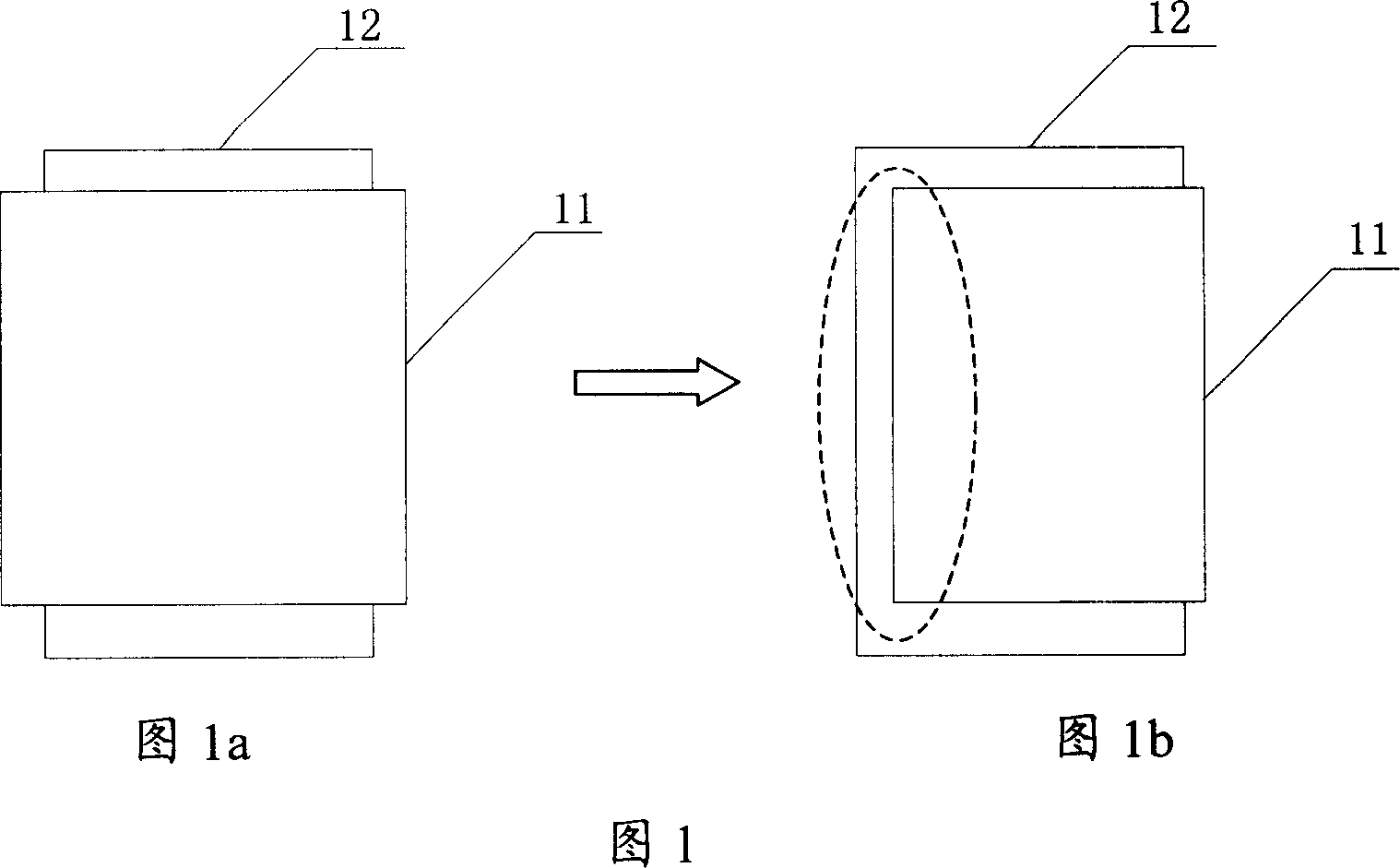
[0045] The core idea of ​​the present invention is: in the process of forming the metal silicide prevention region, the order of the process is improved, and the deep ultraviolet photoresist is removed (strip) before the wet etching process; and by adjusting the thickness of the metal silicide prevention layer, It is ensured that the metal silicide preventing layer in the opening region can be completely removed, and the metal silicide preventing layer in the preventing region can be kept with sufficient thickness. In this way, the fineness of lines required by the 0.16 / 0.18 μm process is met, and the phenomenon of peeling and offset of the photoresist layer does not occur.

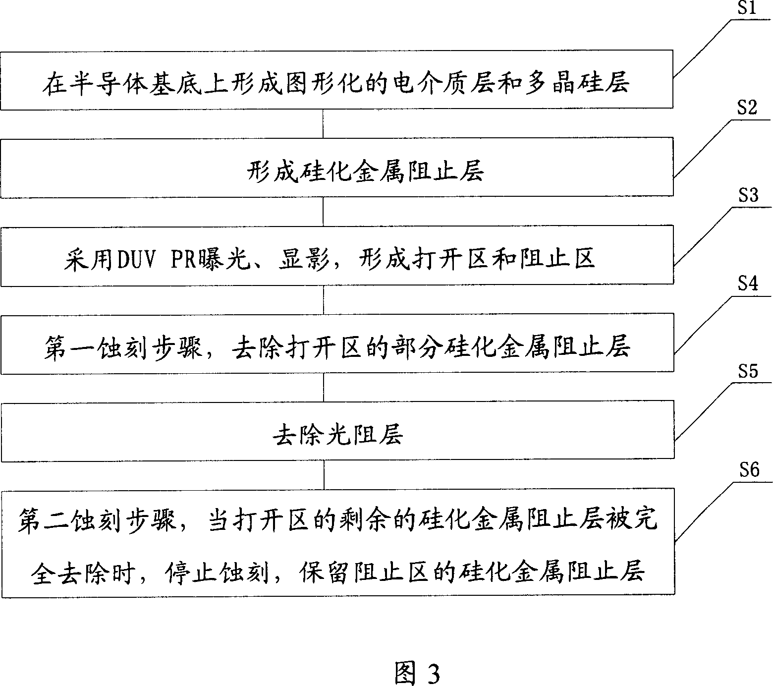
[0046] Referring to FIG. 3 , it shows a flow chart of steps for forming a metal silicide prevention region by using the method of the present invention. Referring to FIG. 4 , it shows a schematic cross-sectional view of the steps of the embodiment shown in FIG. 3 , and FIG. 4 includes FIGS. 4a-4d.

[004...


PUM

PropertyMeasurementUnit
Thicknessaaaaaaaaaa

Abstract

The method includes steps: forming patternized dielectric layer and polycrystalline silicon layer on semiconductor substrate; forming arrestment layer of silicate metal (ALSM); exposing, and developing layer of silicate metal to form unbarred section and arrestment section; the first etching step in use for removing partial ALSM in unbarred section; removing photoresistive layer; second etching step in use for stopping etching to reserve ALSM in arrestment section when residual arrestment layer of silicate metal in unbarred section is removed fully. The invention uses two times of etching steps. Before wet etching process, the second etching step removes deep violet light photoresistive so as to avoid the photoresistive layer from peeling off caused by poor adhesive force. Thus, in procedure for preparing logic circuit in 0.16 / 0.18 micros, the invention makes deep violet light photoresistive adapt photo-etching requirement of more and more thinner.

Description

technical field [0001] The invention relates to a manufacturing process of a semiconductor logic circuit (LG), in particular to a method for forming a metal silicide stop region and a method for manufacturing a low-resistance semiconductor device using the process. Background technique [0002] The photoresist used in the semiconductor manufacturing process is mainly composed of resin, photosensitive agent and solvent. The main function of the resin is to act as a barrier layer during etching or ion implantation; The reacted compound facilitates the development process; the solvent is used to disperse the resin and photosensitive agent evenly, so that the photoresist coating process can proceed smoothly. According to different light sources, photoresists can be divided into three categories: G-line (436nm), I-line (365nm) and Deep UV (193-248nm) (referred to as DUV PR). [0003] With the development of semiconductor technology, G-line photoresist has gradually withdrawn fro...

Claims


Application Information

Patent Timeline
IPC IPC(8): H01L21/3213H01L21/768H01L21/28
Inventor 侯大维周朝锋
Owner SEMICON MFG INT (SHANGHAI) CORP
Why Eureka
Eureka Blog
Learn More