Flash- and rom-memory

A memory cell, RM2 technology, used in flash and read-only (ROM) memory

Inactive Publication Date: 2007-10-17
NXP BV
View PDF3 Cites 5 Cited by
  • Summary
  • Abstract
  • Description
  • Claims
  • Application Information

AI Technical Summary

Problems solved by technology

This may adversely affect the magnitude of the bit line current and peripheral circuits
[0013] More generally, the prior art approach

Method used


Image

  • Flash- and rom-memory
  • Flash- and rom-memory
  • Flash- and rom-memory

Examples


Embodiment Construction

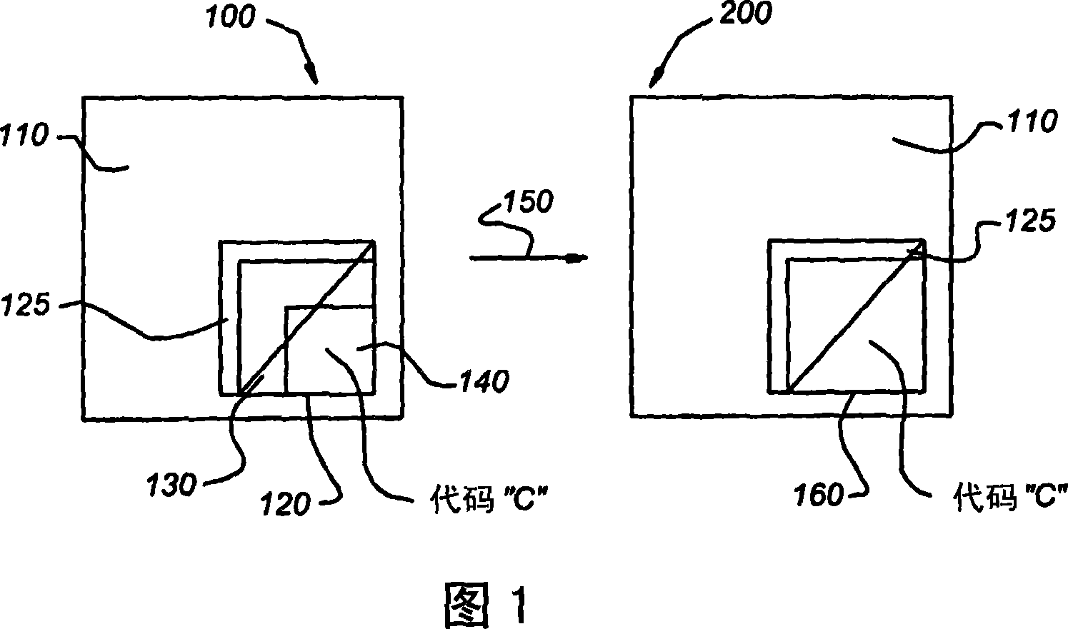
[0054] Figure 1 schematically shows the Flash-ROM conversion of an SOC device.

[0055] The first SOC device 100 includes a device portion 110 produced by baseline technology. Embedded in the device portion 110 is a Flash portion 120 . Symbolically, the wiring scheme between device portion 110 and Flash portion 120 is represented by region 125 . The flash memory part 120 includes a peripheral circuit 130 and a flash memory part 140 . The peripheral circuit 130 is connected to the wiring scheme 125 of the device part 110 at one end and connected to the flash memory part 140 at the other end. The flash memory part 140 includes a plurality of flash memory cells, and the flash memory part 140 is configured to store program code C in the plurality of flash memory cells. The program code C refers to a program that provides functions to the SOC device 100 during operation of the SOC device 100 .

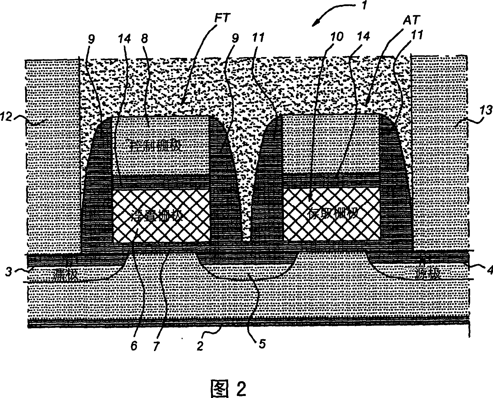
[0056] The peripheral circuit 130 includes a high voltage driving circuit configure...


PUM


Abstract

The present invention provides a method for conversion of a Flash memory cell on a first semiconductor device to a ROM memory cell in a second semiconductor device, the first and second semiconductor device each being arranged on a semiconductor substrate and each comprising an identical device portion and an identical wiring scheme for wiring the device portion to the Flash memory cell and to the ROM memory cell, respectively; the Flash memory cell being made in non-volatile memory technology and comprising an access transistor and a floating transistor, the floating transistor comprising a floating gate and a control gate; the ROM memory cell being made in a baseline technology and comprising a single gate transistor, which method includes manipulating a layout of at least one baseline mask as used in the baseline technology; the manipulation including: incorporating into the layout of the at least one baseline mask a layout of the Flash memory cell, and converting the layout of the Flash memory cell to a layout of one ROM memory cell by eliminating, from the at least one baseline mask, a layout for the floating transistor from the layout of the Flash memory cell and designating the layout of the access transistor of the Flash memory cell as a layout of the single gate transistor of the ROM memory cell.

Description

technical field [0001] The present invention relates to a method for converting flash memory to read-only (ROM) memory. Furthermore, the present invention relates to a semiconductor device including the thus converted ROM memory. Background technique [0002] In current ULSI technology, many semiconductor devices are fabricated as "system-on-chip" (SOC) devices. In such a system-on-chip, initially separately fabricated device structures are combined on a single chip. This allows the incorporation of eg analog, bipolar, (non-volatile) memory and logic CMOS technologies on a small semiconductor area. [0003] Often, the mainstream process of a baseline technology is extended to embed one or more other technologies as an option. Typically, the baseline technology involves CMOS technology, which requires single-level polysilicon fabrication technology. Other technologies requiring multi-layer polysilicon fabrication techniques, such as analog, bipolar and (non-volatile) memo...

Claims


Application Information

Patent Timeline
IPC IPC(8): H01L27/112H01L27/115H01L21/8246H01L21/8247
CPCH01L27/1122H01L27/112H01L27/11226H01L27/115H10B20/00H10B20/30H10B20/34H10B69/00H10B63/80
Inventor 罗伯·费哈尔吉多·J·M·多曼斯毛里茨·斯托姆斯罗格·库彭斯弗朗斯·J·李斯特罗伯特·H·伯泽
Owner NXP BV
Why Eureka
Try Eureka