Full refraction projection optical system

A projection optical system and full refraction technology, applied in the field of projection optical systems, can solve the problems that aberrations cannot meet bumps, do not conform to lithography technology, etc., and achieve the effects of reducing processing, improving imaging quality, and correcting aberrations

Active Publication Date: 2007-10-31
SHANGHAI MICRO ELECTRONICS EQUIP (GRP) CO LTD
View PDF3 Cites 23 Cited by
  • Summary
  • Abstract
  • Description
  • Claims
  • Application Information

AI Technical Summary

Problems solved by technology

The patent gives the data of the objective lens and the imaging quality, but the aberration cannot meet the requirements of the bumping lithography technology at all, and there are two glued surfaces that do not meet the requirements of the lithography technology.

Method used


Image

  • Full refraction projection optical system
  • Full refraction projection optical system

Examples


Embodiment Construction

[0022] The omni-refractive projection optical system of the present invention will be further described in detail below.

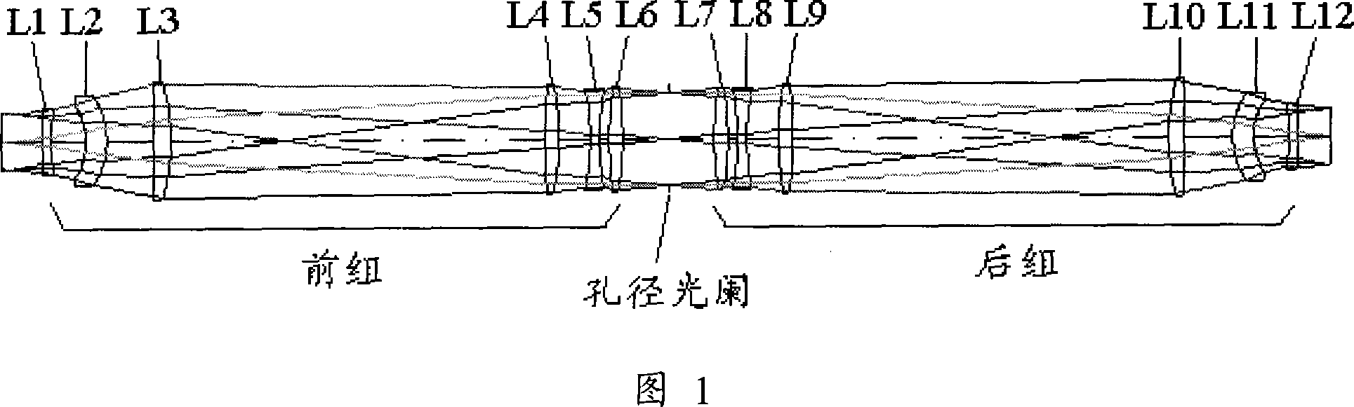
[0023] The present invention provides a total refraction projection optical system. As shown in FIG. 1, the projection optical system has a symmetrical structure, that is, it includes a front group, an aperture stop, and a rear group sequentially from the side of the object plane, and the front group and Each lens component of the rear group takes the aperture stop surface as the symmetry plane, and the optical structure is completely symmetrical (the surface radius and interval are equal, and the optical material is consistent), and the magnification is -1. The advantage of the symmetrical structure with a magnification of -1 is that according to the primary aberration theory, the vertical axis aberrations: coma, distortion, and chromatic aberration of magnification are automatically corrected to 0, and then the axial aberrations are corrected separately b...


PUM


Abstract

This invention provides one total reflection projection optical system for object plane to form imaging plane, wherein the said system is divided into front and back sets to form hole diaphragm as symmetric surfaces; the front set comprises first to sixth lens with one to three lens form reverse distant structure; the back set orderly comprises seven to twelve lens symmetric to six to one lens about hole radium; the said whole reflection projection optical system all surface types are of sphere or plane without non-sphere surface.

Description

technical field [0001] The invention relates to a projection optical system, in particular to a total refraction projection optical system used for semiconductor photolithography and photographic plate making. Background technique [0002] With the development of projection lithography technology, the performance of projection optical system is gradually improved, and can be applied to various fields such as integrated circuit manufacturing. Projection lithography technology has been successfully applied to the field of submicron resolution integrated circuit manufacturing. In semiconductor packaging technology, projection lithography technology can be used for gold bumps / tin bumps that require lower resolution (such as a few microns), larger depth of focus, and higher yields, and silicon wafer-level chip-scale packaging (WLCSP) technology and other fields. [0003] However, in the prior art, such as U.S. Patent No. 6,879,383 (announcement date: April 12, 2005), it adopts ...

Claims


Application Information

Patent Timeline
Patent Type & Authority Applications(China)
IPC IPC(8): G02B13/00G02B9/04G02B1/02
Inventor 蔡燕民
Owner SHANGHAI MICRO ELECTRONICS EQUIP (GRP) CO LTD
Why Eureka
Try Eureka