Semiconductor laser device and method for fabricating the same

A technology of a laser device and a manufacturing method, which can be applied to semiconductor laser devices, semiconductor lasers, laser devices, etc., can solve problems such as difficulty in ensuring high yield

Inactive Publication Date: 2007-10-31
PANASONIC CORP
View PDF0 Cites 10 Cited by
  • Summary
  • Abstract
  • Description
  • Claims
  • Application Information

AI Technical Summary

Problems solved by technology

[0017] However, as described above, it is difficult to ensure a high yield when fabricating a monolithic two-wavelength semiconductor laser device using the method disclosed in Patent Document 1.

Method used


Image

  • Semiconductor laser device and method for fabricating the same
  • Semiconductor laser device and method for fabricating the same
  • Semiconductor laser device and method for fabricating the same

Examples


Embodiment Construction

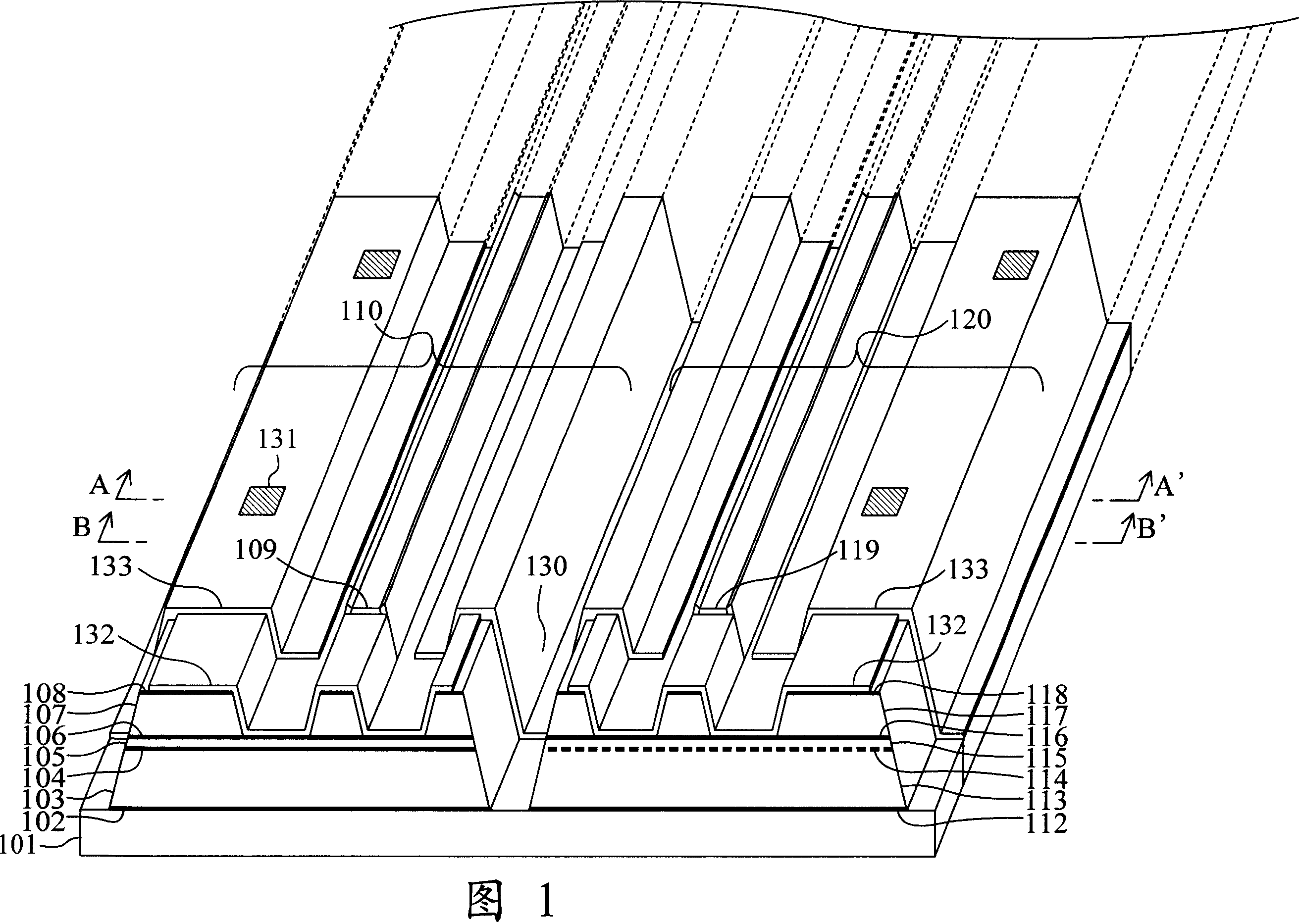
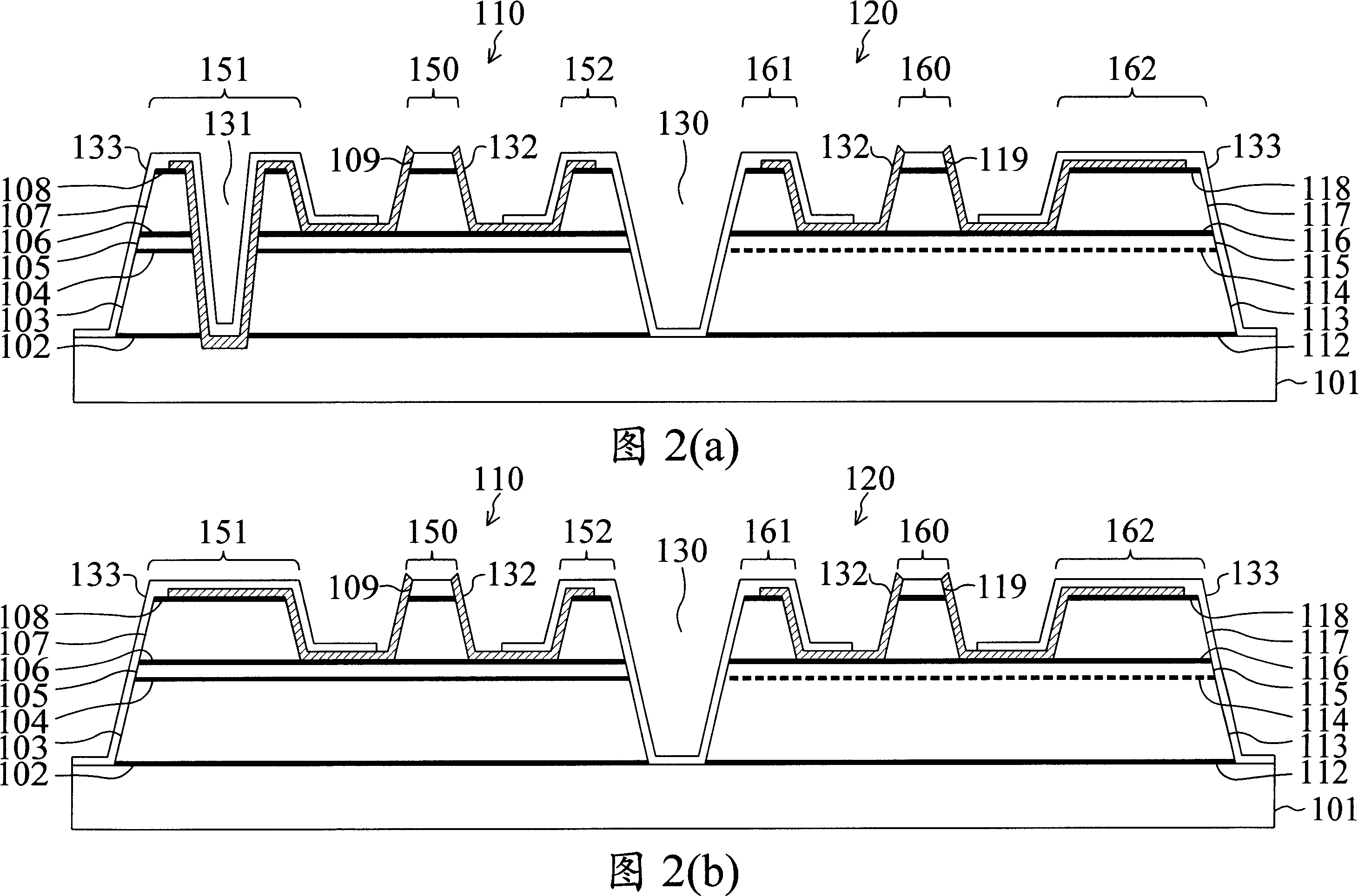
[0089] Next, a semiconductor laser device according to an embodiment of the present invention, specifically, a monolithic two-wavelength semiconductor laser device and a manufacturing method thereof will be described with reference to the drawings.

[0090] (Structure of a two-wavelength semiconductor laser device)

[0091] Fig. 1 is a perspective view showing the structure of the semiconductor laser device involved in this embodiment, and Fig. 2(a) is a cross-sectional view of line A-A' in Fig. sectional view), Fig. 2(b) is a sectional view of line B-B' in Fig. 1 (the sectional view without crossing the above-mentioned cavity).

[0092] As shown in Fig. 1 and Fig. 2(a), Fig. 2(b), the monolithic dual-wavelength semiconductor laser device of this embodiment has an infrared light on a substrate 101 made of n-type gallium arsenide (GaAs), for example. The structure of the laser element 110 and the red laser element 120 is as follows.

[0093] First, the infrared laser element ...


PUM


Abstract

The present invention provides a monolithic multiple-wavelength semiconductor laser device capable of achieving a high yield, and provides a method of manufacturing the same. An infrared laser device 110 and red laser device 120 are formed on the same substrate 101. Each of the laser elements 110, 120 is provided with a double heterostructure composed by laminating an n-type cladding layer 103 or 113, an active layer 104 or 114, and a p-type first cladding layer 105 or 115 in that order; and a ridge-shaped waveguide 150 or 160 including a p-type second cladding layer 107 or 117, and a p-type contact layer 109 or 209 provided on the p-type second cladding layer. A current blocking layer 132 is formed on both side-walls of each ridge-shaped waveguide 150, 160 and around them. A leakage preventing layer 133 is formed on the current blocking layer 132.

Description

technical field [0001] The present invention relates to a semiconductor laser device and a manufacturing method thereof, in particular to a multi-wavelength semiconductor laser device having a monolithic structure composed of a plurality of semiconductor laser elements having different oscillation wavelengths and a manufacturing method thereof. Background technique [0002] In recent years, in various fields including video players, digital video disc (DVD) drives for recording and reproducing optical information characterized by a large storage capacity are rapidly spreading. In addition, it is urgently desired that the same device can also be used to read from conventionally used compact discs (CD), recordable discs (CD-R), and erasable and rewritable discs (CD-RW). For this reason, as a light source for a digital video disc or an optical pickup for optical disc recording and reproduction, a red semiconductor laser element with a wavelength of 650 nanometers for a digital ...

Claims


Application Information

Patent Timeline
Patent Type & Authority Applications(China)
IPC IPC(8): H01S5/40H01S5/32H01S5/22
CPCH01S5/2214H01S5/16H01S5/4087H01S5/4031H01S5/22H01S3/0941H01S5/00
Inventor 鹿岛孝之牧田幸治
Owner PANASONIC CORP
Why Eureka
Try Eureka