Silicon based titanium dioxide electroluminescent device and method for producing the same

An electroluminescent device, titanium dioxide technology, applied in electrical components, semiconductor devices, circuits, etc., to achieve the effect of simple structure and implementation

Inactive Publication Date: 2008-01-02
ZHEJIANG UNIV
View PDF0 Cites 4 Cited by
  • Summary
  • Abstract
  • Description
  • Claims
  • Application Information

AI Technical Summary

Problems solved by technology

However, the electroluminescence of silicon-based titania on silicon substrates has not been realized so far.

Method used


Image

  • Silicon based titanium dioxide electroluminescent device and method for producing the same

Examples


Embodiment 1

[0016] Take the following process steps: 1) Clean P-type with a resistivity of 0.005 ohm cm and a size of 15×15mm 2 , a silicon wafer with a thickness of 675 microns, after cleaning, put it into the reaction chamber of the DC reactive magnetron sputtering device, and the vacuum degree of the reaction chamber is pumped to 5×10 -3 Pa; Deposit TiO with a thickness of about 100nm on a silicon wafer by reactive DC sputtering 2 When sputtering the thin film, a Ti metal target with a purity of 99.9% is used, the substrate temperature is 100°C, the sputtering power is 70W, and the 2 Mixed gas with Ar, O 2 The flow ratio of Ar and Ar is 1:3, and the working pressure is 0.7Pa; 2) in TiO 2 A 50nm-thick ITO electrode is sputtered on the film, and a 100nm-thick Al is deposited on the back of the silicon as an ohmic contact electrode, both of which have an area of ​​10×10mm 2 .

Embodiment 2

[0017] Embodiment 2 takes the following process steps: 1) cleaning N-type , with a resistivity of 0.5 ohm cm and a size of 15×15mm 2 , a silicon wafer with a thickness of 675 microns, after cleaning, put it into the reaction chamber of the DC reactive magnetron sputtering device, and the vacuum degree of the reaction chamber is pumped to 5×10 -3 Pa; Deposit TiO with a thickness of about 200nm on a silicon wafer by reactive DC sputtering 2 Thin films, when sputtering, use a Ti metal target with a purity of 99.9%, a substrate temperature of 300°C, a sputtering power of 100W, and an O 2 Mixed gas with Ar, O 2 The flow ratio with Ar is 1:2, and the working pressure is 5Pa; 2) in TiO 2 A 50nm-thick ITO electrode is sputtered on the film, and a 100nm-thick Au is deposited on the back of the silicon as an ohmic contact electrode, both of which have an area of ​​10×10mm 2 .

Embodiment 3

[0019] Take the following process steps: 1) Clean P-type with a resistivity of 50 ohm.cm and a size of 15×15mm 2 , a silicon wafer with a thickness of 675 microns, after cleaning, put it into the reaction chamber of the DC reactive magnetron sputtering device, and the vacuum degree of the reaction chamber is pumped to 5×10 -3 Pa; Deposit TiO with a thickness of about 150nm on a silicon wafer by reactive DC sputtering 2 Thin films, when sputtering, use a Ti metal target with a purity of 99.9%, a substrate temperature of 400°C, a sputtering power of 120W, and an O 2 Mixed gas with Ar, O 2 The flow ratio with Ar is 1:1, and the working pressure is 10Pa; 2) in TiO 2 A 50nm-thick ITO electrode is sputtered on the film, and a 100nm-thick Al is deposited on the back of the silicon as an ohmic contact electrode, both of which have an area of ​​10×10mm 2 .

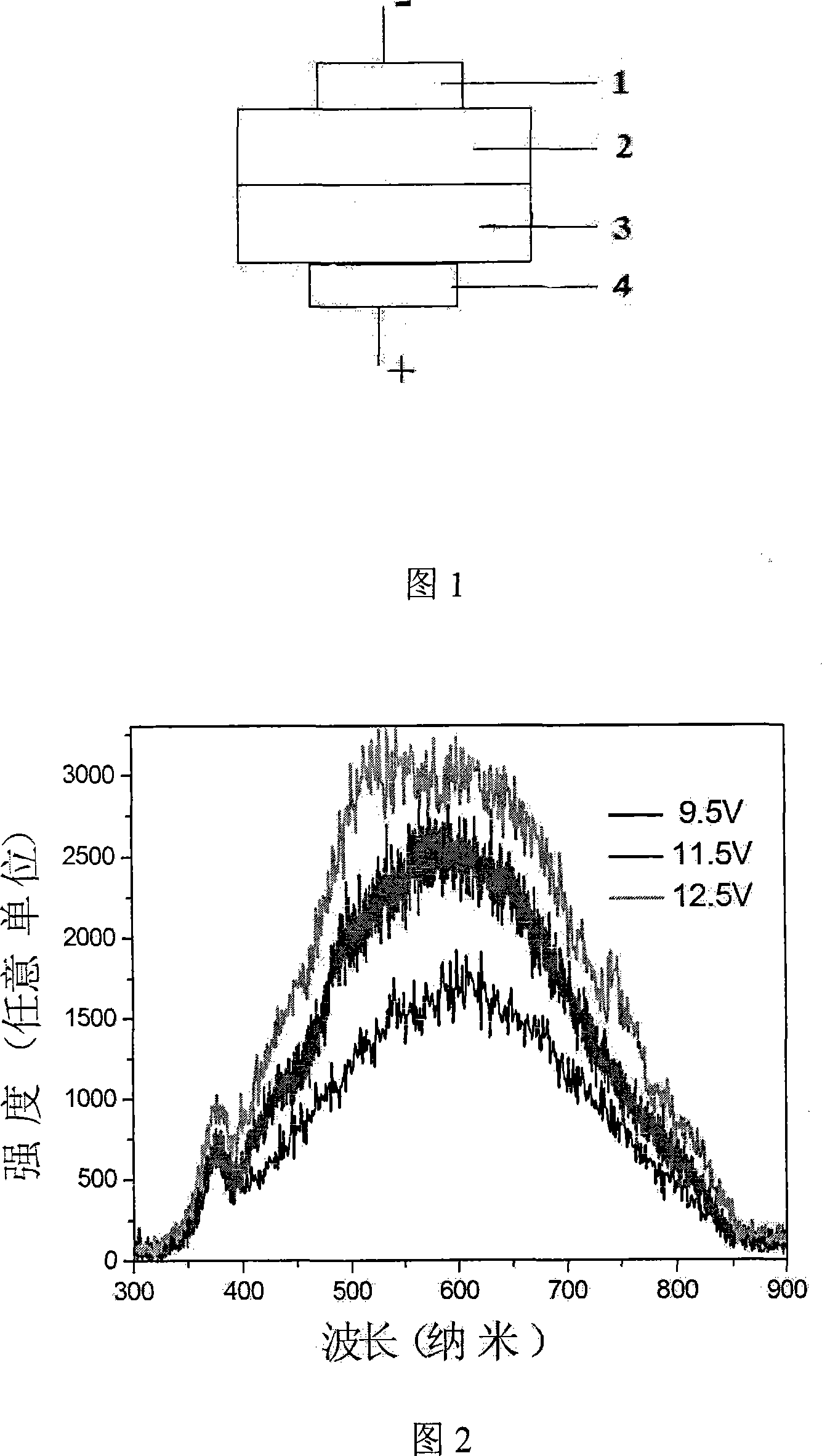
[0020] Figure 2 shows the electroluminescence (EL) spectra of the device obtained by the above method measured at room tempe...


PUM

PropertyMeasurementUnit
electrical resistivityaaaaaaaaaa

Abstract

The invention discloses a silicon-base titania electroluminescent device, wherein the front face of the silicon substrate is deposited with a TiO2 film and a transparent ITO electrode from down to up, the back of the silicon substrate is deposited with a Ohm contact electrode. And the preparation comprises that first washing P-type or N-type silicon slice to be input into a reaction room of direct-current reaction magnetic-control splash device, vacuuming the reaction room, using pure titanium metal as target, using O2 and Ar as splash gas, to process splash deposition to obtain a TiO2 film, then splashing an ITO electrode on the TiO2 film, depositing an Ohm contact electrode at the back of the silicon substrate. The invention has simple structure and preparation, while the electroluminescent lighting peak is around 370nm and 600nm. The preparation is compatible with prior silicon device plane art, which support the batch production with low cost.

Description

technical field [0001] The invention relates to a silicon-based titanium dioxide electroluminescent device and a preparation method thereof. Background technique [0002] Titanium dioxide is a wide bandgap semiconductor with a bandgap width of 3-3.2ev. Titanium dioxide has a relatively low phonon energy, which reduces the chance of non-radiative transitions. In addition, it also has properties such as photoelectric conversion and optical nonlinearity. These superior properties make titanium dioxide much attention. In 1983, the Nakato.Y group obtained the electroluminescence of titanium dioxide for the first time by solution method (references: Nakato Y, Tsumura A and Tsubomura H, J.Phys.Chem 87(1983) 2402). Afterwards, Tomoaki Houzouji et al. used an improved solution method to obtain relatively high-strength TiO 2 (References: Tomoaki Houzouji, Nobuhiro Saito, Akihiko Kudo, and Tadayoshi Sakata, Chemical Physics Letters 254 (1996) 109). However, the devices prepared by...

Claims


Application Information

Patent Timeline
Patent Type & Authority Applications(China)
IPC IPC(8): H01L33/00
Inventor 杨德仁马向阳章圆圆陈培良阙端麟
Owner ZHEJIANG UNIV
Why Eureka
Try Eureka