Transparent conductive film forming apparatus, multilayer transparent conductive film continuously forming apparatus and method of film forming therewith

A transparent conductive film and deposition technology, applied in coatings, circuits, photovoltaic power generation, etc., can solve the problems of low substrate speed, increased nozzle temperature, low use efficiency of raw materials, etc., to reduce the necessity of maintenance, improve The effect of using efficiency

Active Publication Date: 2008-01-16
太阳能先锋株式会社
View PDF3 Cites 3 Cited by
  • Summary
  • Abstract
  • Description
  • Claims
  • Application Information

AI Technical Summary

Problems solved by technology

Has the problem of raising the temperature of the nozzle during growth due to heat radiated from the heating plate, and deposits build up on the nozzle, so nozzle maintenance is necessary
Furthermore, there is the problem that, due to the nozzle structure of the prior art having a space between the injection parts for the organometallic compound, water and diborane, the product appears on the back side of the nozzle or even on the upper part of the chamber build-up, resulting in inefficient use of raw materials and the need for frequent maintenance
Therefore, there is a problem that in the case where the heating plate has uneven heat distribution, a transparent conductive film with uneven sheet resistance etc. is formed
[0013] 3. The device has only one chamber
Therefore there is such a problem that the speed of substrate processing is low, and the speed of film deposition is low

Method used


Image

  • Transparent conductive film forming apparatus, multilayer transparent conductive film continuously forming apparatus and method of film forming therewith
  • Transparent conductive film forming apparatus, multilayer transparent conductive film continuously forming apparatus and method of film forming therewith
  • Transparent conductive film forming apparatus, multilayer transparent conductive film continuously forming apparatus and method of film forming therewith

Examples


Embodiment Construction

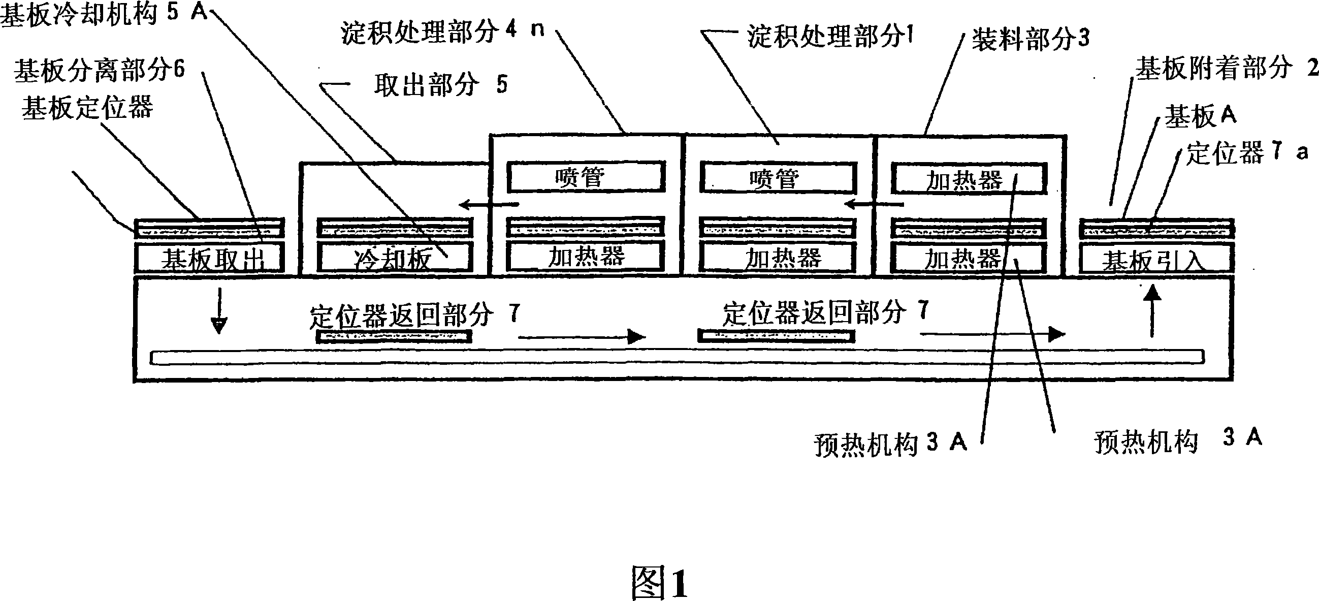
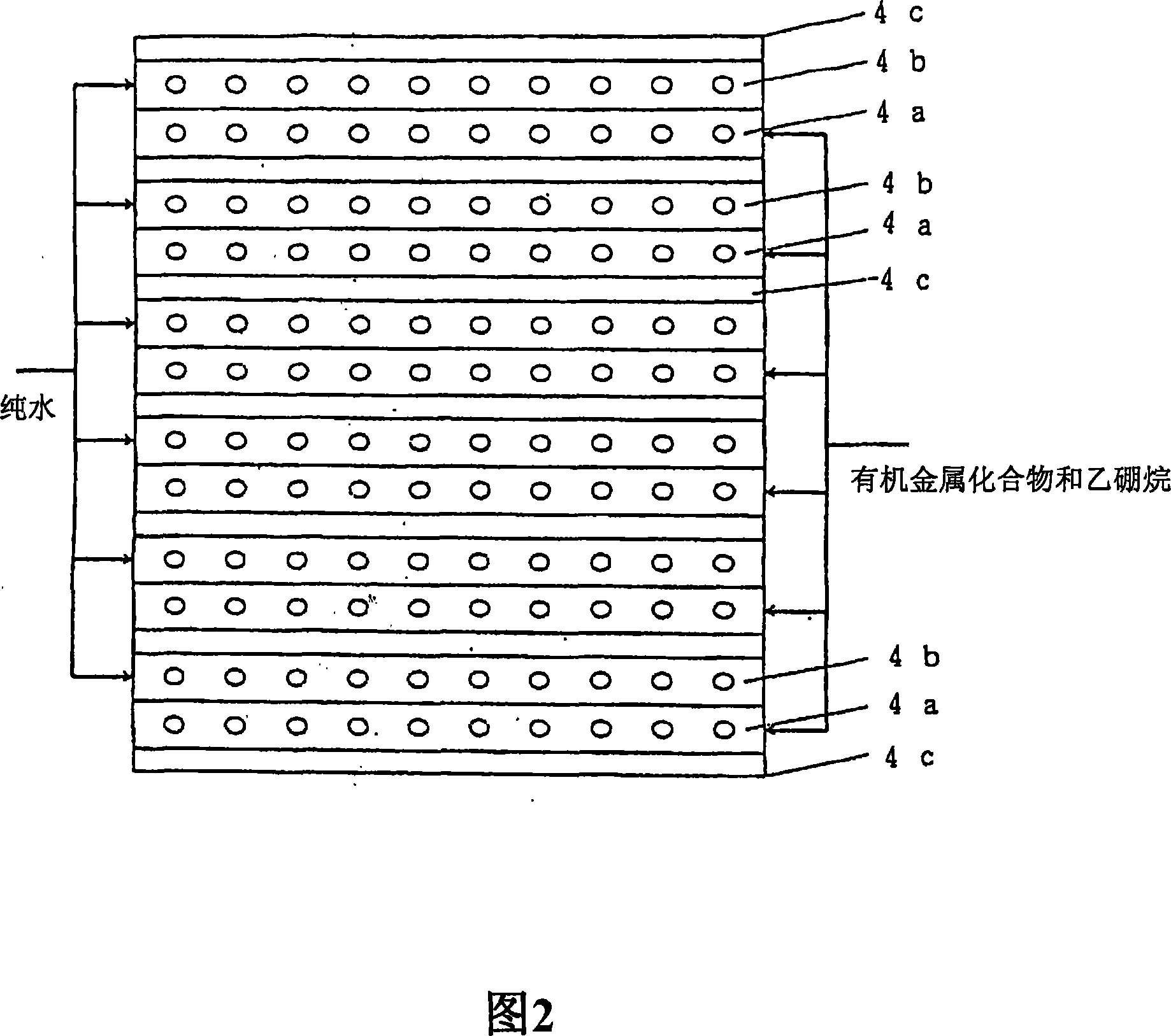
[0054] The present invention provides a film deposition apparatus for continuously forming a multilayer transparent conductive film including multiple layers of n-type semiconductors on a substrate and a method of forming the multilayer transparent conductive film. As shown in FIG. 1, the apparatus includes: a substrate attaching section 2, where a substrate A is attached to a positioner 7a in air; a loading section 3, where evacuation is performed; a multilayer deposition processing section 4, which includes two One or more deposition processing sections (41 to 4n) are used for heating the substrate by adding an organometallic compound (diethylzinc Zn(C 2 h 5 ) 2 ), diborane (B 2 h 6 ) and water (water vapor) react in the vapor phase, and use metal organic chemical vapor deposition (MOCVD) method to form a transparent conductive film comprising n-type semiconductor (such as ZnO) on the heated substrate; take out part 5, in Here, the substrate with the multilayer transpare...


PUM


Abstract

It is intended to attain an increase of film forming rate while saving raw materials and while maintaining a homogeneous high film quality. There is provided a multilayer transparent conductive film continuously forming apparatus, comprising a substrate mounting section; a charging section adapted for vacuum exhaust; a multilayer film forming treatment section including multiple film forming treatment areas capable of carrying out reaction of an organometallic compound (diethylzinc), diborane and water in a vapor phase and forming a transparent conductive film on a substrate according to the MOCVD process; a substrate ejection section; a substrate detaching section; and a setter return section capable of returning a substrate setter to the substrate mounting section, wherein while sequentially traveling the mentioned sections, a multilayer transparent conductive film is continuously formed on the substrate. Each of the film forming treatment areas is fitted with respective nozzles for injection of the organometallic compound, diborane and water and further fitted with cooling means for cooling them.

Description

technical field [0001] The present invention relates to a film deposition apparatus and a film forming method for continuously forming a transparent conductive film having a multilayer structure by an MOCVD method. Background technique [0002] In the step of forming a transparent conductive film in the solar cell production steps, a sputtering method and a metal organic chemical vapor deposition (MOCVD) method are used. The reaction in the MOCVD method is performed at a low temperature (200° C. or lower), and the method is a chemical vapor deposition method. Thus, the MOCVD method is a gentle film deposition method that does not induce mechanical damage to other thin constituent layers, unlike techniques such as sputtering methods where bombardment of energetic particles damages underlying thin constituent layers. [0003] In producing a CIGS type thin film solar cell, a transparent conductive film is formed on a thin constituent layer on the light incident side thereof. ...

Claims


Application Information

Patent Timeline
Patent Type & Authority Applications(China)
IPC IPC(8): H01L21/205C23C16/40C23C16/455C23C16/46H01B13/00H01L51/42
CPCH01L21/02576H01L21/365C23C16/407H01L21/02554C23C16/45574C23C16/54H01L21/0262C23C16/45578Y02E10/50H01L31/1884C23C16/45572Y02E10/541Y02E10/549C23C16/40H01L31/04C23C16/455H10K30/00
Inventor 田中良明
Owner 太阳能先锋株式会社
Why Eureka
Try Eureka