Layered thin film structure, layered thin film forming method, film forming system and storage medium

A technology of laminated structure and film, applied in the direction of coating, thin material processing, transportation and packaging, can solve the problems of inability to increase the height, difficult to meet the requirements of step coverage, insufficient adhesion, etc., to achieve high adhesion, restraint Film peeling, improved step coverage

Inactive Publication Date: 2008-01-30
TOKYO ELECTRON LTD
View PDF1 Cites 0 Cited by
  • Summary
  • Abstract
  • Description
  • Claims
  • Application Information

AI Technical Summary

Problems solved by technology

[0006] However, as described above, the copper alloy film is formed by the sputtering process, and in the film formation by the sputtering process, step coverage is difficult especially in view of today's design rules where the line width and the like are more miniaturized. Satisfies the requirements, but there is a problem that the concave part of the wafer surface cannot be filled sufficiently
[0007] In addition, in the case where the deposited copper alloy film is to be formed at a predetermined site, such as the boundary with the base layer, in a state where the concentration of the alloy species is higher than that of other parts, because the copper alloy film The concentration of the alloy species in the copper alloy film is determined by the concentration of the alloy species in the pre-manufactured metal target, and the concentration of the alloy species cannot be changed in the sputtering film formation, so it is impossible to make the concentration of the alloy species in the copper alloy film only in the Concentration control such that specific parts become higher
Therefore, the migration cannot be sufficiently suppressed, so that sufficient adhesion cannot be obtained, and the occurrence of film peeling cannot be prevented.
[0008] Therefore, it is considered to form the above-mentioned copper alloy film by CVD (Chemical Vapor Deposition: Chemical Vapor Deposition) instead of sputtering. In this case, there is a problem that only one kind of metal film can be formed at a time, and only The CVD method cannot uniformly mix or disperse the metal atoms of the alloy species into the film as a whole

Method used


Image

  • Layered thin film structure, layered thin film forming method, film forming system and storage medium
  • Layered thin film structure, layered thin film forming method, film forming system and storage medium
  • Layered thin film structure, layered thin film forming method, film forming system and storage medium

Examples


Embodiment Construction

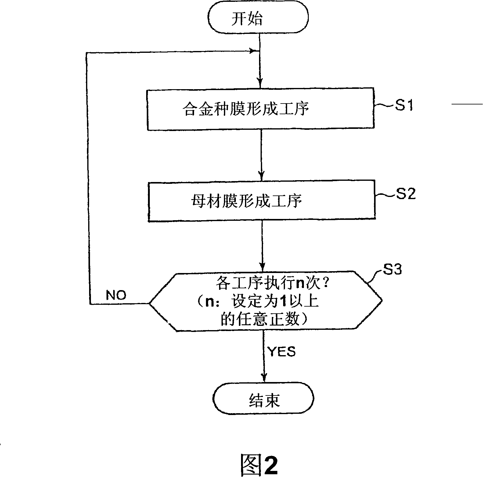
[0034] Hereinafter, an embodiment of the multilayer structure of the thin film, its forming method, film forming apparatus, and storage medium of the present invention will be described with reference to the drawings.

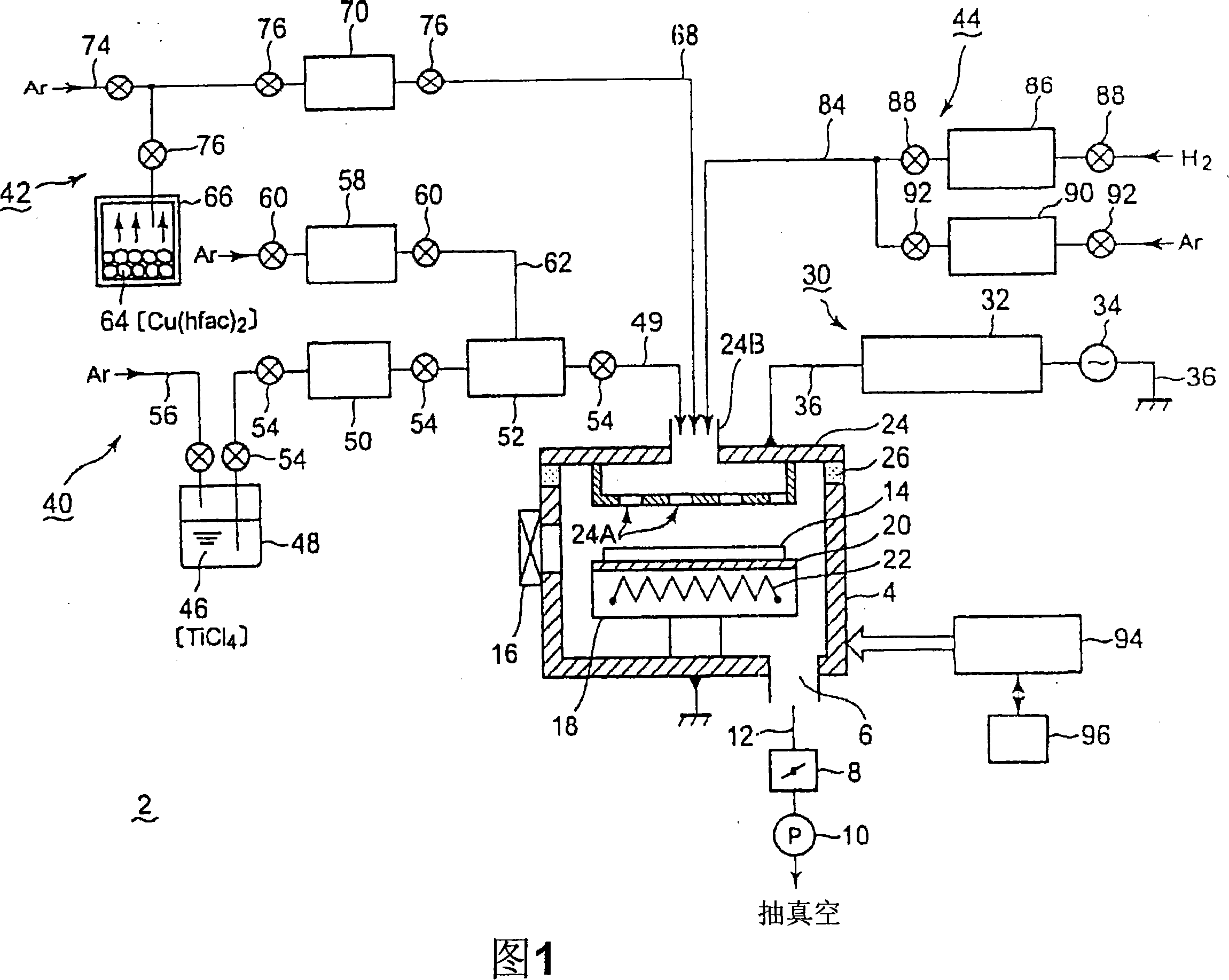
[0035] FIG. 1 is a schematic configuration diagram showing an example of a film forming apparatus of the present invention.

[0036]First, the film forming apparatus 2 of the present invention will be described. The film forming apparatus 2 has a cylindrical processing container 4 formed of, for example, aluminum or the like. The processing container 4 is grounded, and an exhaust port 6 is formed at the bottom thereof. A vacuum exhaust system 12 provided with a pressure control valve 8 and a vacuum pump 10 in the middle is connected to the exhaust port 6, and can vacuum the inside of the processing container 4 and set it to an arbitrary pressure.

[0037] In addition, a gate valve 16 is provided on the side wall of the processing container 4 to open and close ...


PUM


Abstract

The present invention provides a multilayer structure of a thin film that has high adhesion to the substrate, can suppress the occurrence of film peeling, can sufficiently improve the step coverage even if the miniaturization is further developed, and can sufficiently diffuse elements of the alloy species. form method. In this method, multiple layers of thin films are deposited on the surface of the object to be processed in a vacuumable processing container (4) to form a laminated structure of thin films, and the following steps are alternately carried out more than once: A raw material gas of the first metal and a reducing gas, an alloy seed film forming step of forming an alloy seed film (104) composed of the first metal; and a raw material gas containing a second metal different from the above-mentioned first metal as a base material and a reducing gas to form a base material film (106) made of a second metal thicker than the alloy seed film.

Description

technical field [0001] The present invention relates to a laminated structure of a thin film formed on the surface of an object to be processed such as a semiconductor wafer, its forming method, a film forming device for implementing the method, and a storage medium storing a program for controlling the film forming device. Background technique [0002] Generally, in order to manufacture semiconductor integrated circuits such as ICs and LSIs, film formation processing, etching processing, oxidation diffusion processing, annealing processing, modification processing, etc. are repeatedly performed on a processing object such as a semiconductor wafer. Recently, due to demands for higher integration, higher miniaturization, and higher operating speed, etc., thinner wiring layers and the like and miniaturization of line widths have been advanced. Under such circumstances, it has been proposed to replace the existing aluminum wiring with copper wiring having a lower resistance (fo...

Claims


Application Information

Patent Timeline
Patent Type & Authority Applications(China)
IPC IPC(8): C23C16/44
CPCC23C16/45542C23C16/06C23C16/45529Y10T428/24975Y10T428/2495C23C16/45553C23C16/52
Inventor 吉井直树小岛康彦佐藤浩
Owner TOKYO ELECTRON LTD
Why Eureka
Try Eureka