Method for forming shallow groove separation structure and shallow groove separation structure

An isolation structure, shallow trench technology, applied in electrical components, semiconductor/solid-state device manufacturing, circuits, etc., can solve problems such as affecting carrier concentration, increasing leakage current, and changing carrier mobility, to improve electrical performance effect

Active Publication Date: 2008-02-13
SEMICON MFG INT (SHANGHAI) CORP +1
View PDF4 Cites 21 Cited by
  • Summary
  • Abstract
  • Description
  • Claims
  • Application Information

AI Technical Summary

Problems solved by technology

[0004] However, since the insulating medium filled in the trench by the HDP-CVD process is very dense, the insulating medium itself will generate strong compressive stress (compressive stress), although the trench sidewall and liner materials are different from the insulating medium filled in the trench. The stress between the dielectrics can be reduced or eliminated by the above methods, but the compressive stress generated by the insulating dielectric itself still exists, so that the shallow trench isolation structure presents a high compressive stress state
When the feature size of the device enters the process node of 65nm and below, the density of components becomes higher and higher, and the space distance between components becomes very small. This stress will change the trench of NMOS and PMOS on both sides of the trench. The lattice structure of the channel affects the carrier concentration, resulting in a change in the mobility of the carrier, thereby increasing the chance of leakage current

Method used


Image

  • Method for forming shallow groove separation structure and shallow groove separation structure
  • Method for forming shallow groove separation structure and shallow groove separation structure
  • Method for forming shallow groove separation structure and shallow groove separation structure

Examples


Embodiment Construction

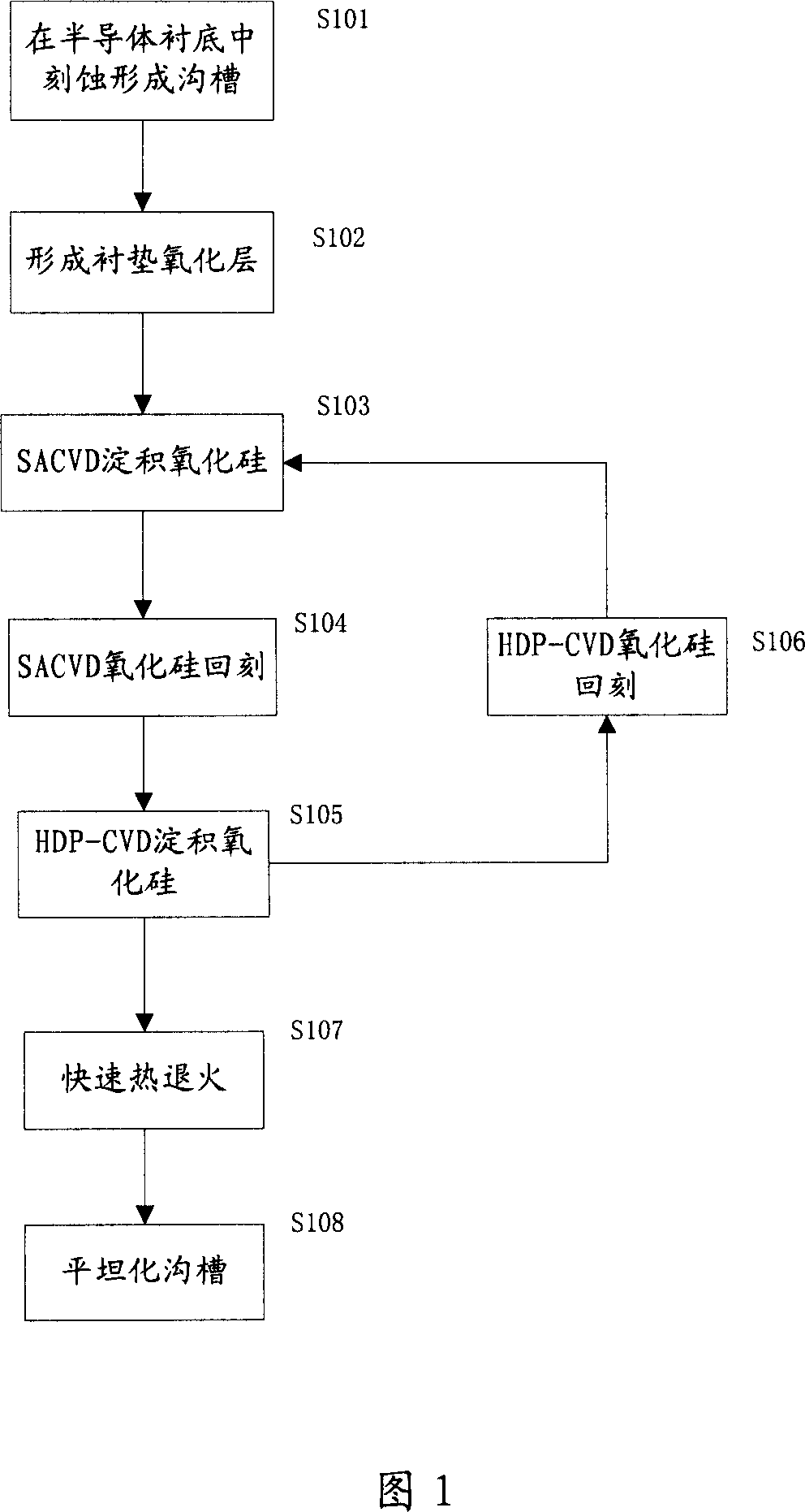
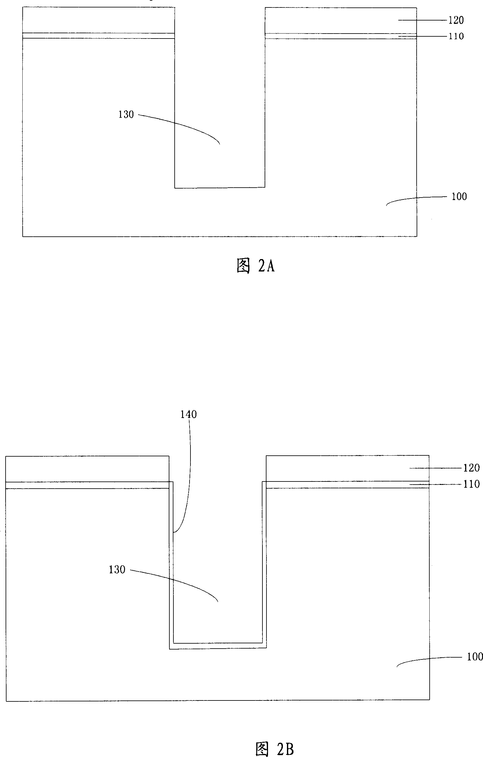
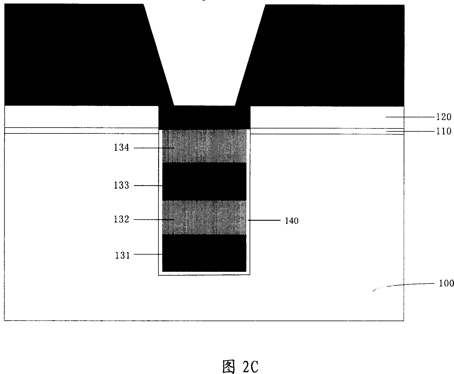
[0065] In order to make the above objects, features and advantages of the present invention more comprehensible, specific implementations of the present invention will be described in detail below in conjunction with the accompanying drawings.

[0066] The invention relates to the technical field of semiconductor integrated circuit manufacturing, in particular to a method for forming a shallow trench isolation structure in a semiconductor device and the shallow trench isolation structure. It should be noted here that this specification provides different embodiments to illustrate the various features of the present invention, but these embodiments are only for convenience of description by using specific compositions and structures, and are not intended to limit this aspect.

[0067] After the manufacturing process of semiconductor devices enters the process node of 65nm and below, the influence of stress on the carrier mobility of CMOS devices becomes more and more obvious. T...


PUM


Abstract

A method for forming shallow groove isolation in semi-conductor device comprises that: a mask film layer is formed on the underlayer of the semi-conductor; the mask film layer is made into a design to expose the underlayer of semi-conductor opposite to the position of the groove; the underlayer is corroded to form a groove and a padding oxidizing layer in the groove; a first insulating medium and a second insulating medium are deposited in turn until the groove is filled fully; a quick flash annealing process is carried out onto the underlayer of the semi-conductor; the insulating mediums are made flat to form a shallow groove isolation structure. The shallow groove isolation structure of the invention comprises the underlayer of the semi-conductor and the grooved formed in the underlayer. The groove is filled with insulating mediums, comprising the first insulating medium and the second insulating medium. The first insulating medium and the second insulating medium are piled against each other, forming a stack structure. The invention effectively controls the stress of the shallow groove isolation structure, thus improving the properties of semi-conductor devices.

Description

technical field [0001] The invention relates to the technical field of semiconductor manufacturing, in particular to a method for forming a shallow trench isolation structure in a semiconductor device and the shallow trench isolation structure. Background technique [0002] As the semiconductor process enters the deep submicron era, in components below 0.13 μm such as CMOS devices, the isolation layer between the NMOS transistor and the PMOS transistor is formed by a shallow trench isolation process (STI). In this process, shallow trenches are first formed on the substrate, and the elements are separated by etched shallow trenches, and then oxide liners are formed on the side walls and bottom of the trenches, and then chemical vapor deposition (CVD ) filling the shallow trench with an insulating medium, such as silicon oxide. After filling the insulating medium, the groove surface is planarized by chemical mechanical polishing (CMP). [0003] In the manufacturing process o...

Claims


Application Information

Patent Timeline
Patent Type & Authority Applications(China)
IPC IPC(8): H01L21/762
Inventor 刘明源吴汉明郭佳衢郑春生
Owner SEMICON MFG INT (SHANGHAI) CORP
Why Eureka
Try Eureka