Ti Hz quanta cascaded semiconductor laser material and its growth method

A technology of quantum cascade, growth method, applied in the field of semiconductor

Inactive Publication Date: 2008-02-20
INST OF SEMICONDUCTORS - CHINESE ACAD OF SCI
View PDF0 Cites 9 Cited by
  • Summary
  • Abstract
  • Description
  • Claims
  • Application Information

AI Technical Summary

Problems solved by technology

Due to the inherent structure of the material,...

Method used


Image

  • Ti Hz quanta cascaded semiconductor laser material and its growth method
  • Ti Hz quanta cascaded semiconductor laser material and its growth method
  • Ti Hz quanta cascaded semiconductor laser material and its growth method

Examples


Embodiment Construction

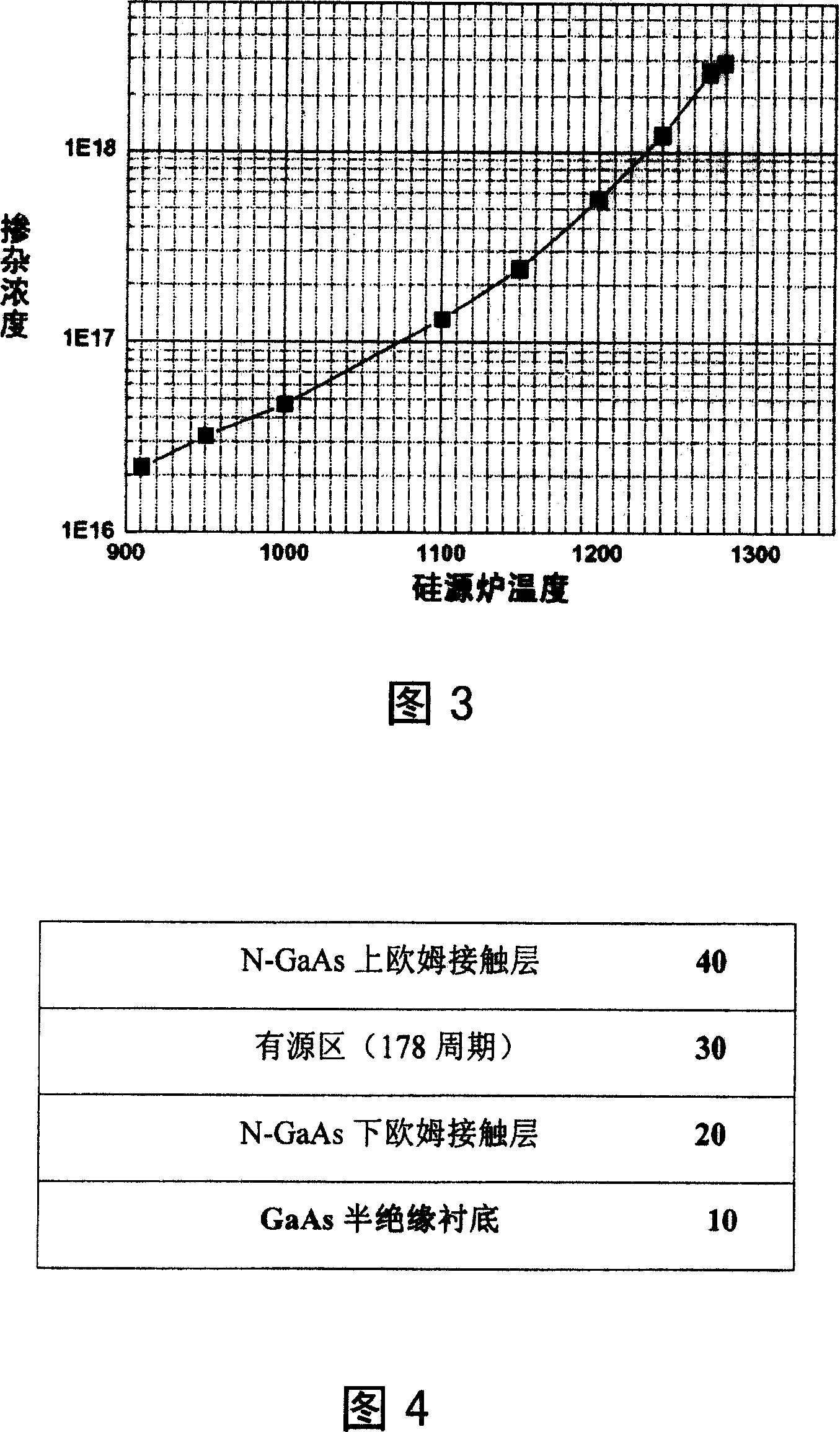
[0038] Please refer to Fig. 4, a method for growing a terahertz quantum cascade semiconductor laser material according to the present invention includes the following growth steps:

[0039] Step 1: take half of the insulating gallium arsenide substrate 10; before growing each layer on the semi-insulating gallium arsenide substrate 10, the aluminum and gallium beam current values ​​under the set growth rate and material composition should be determined, The method is to measure the thickness of the AlGaAs epitaxial layer that meets the design composition, and obtain the corresponding growth rate of AlGaAs under the aluminum and gallium beams after dividing the epitaxial layer, and then obtain the growth rate of GaAs according to the proportional relationship, and then obtain Corresponding beam current value;

[0040] Step 2: using molecular beam epitaxy to grow an N-type gallium arsenide lower ohmic contact layer 20 on the semi-insulating gallium arsenide substrate 10 to make a...


PUM


Abstract

The utility model relates to a growth method of a THz quantum stage linked semiconductor laser material, which is characterized in comprising the following growth steps: step 1: A semiinsulating gallium arsenide substrate is adopted; step 2: N-shaped ohmic contact layer under the gallium arsenide is grown on the semiinsulating gallium arsenide substrate via the use of the molecular rays epitaxial technique to make a lower ohmic electrode; step 3: An active area is grown on the lower ohmic contact layer to form a luminous zone; step 4: An N-shaped gallium arsenide upper ohmic contact layer is grown on the active area to make a lower ohmic electrode to accomplish the growth of the THz quantum stage linked semiconductor laser material.

Description

technical field [0001] The invention relates to the field of semiconductor technology, in particular to a gallium arsenide (GaAs)-based gallium arsenide / aluminum gallium arsenide (GaAs / AlGaAs) terahertz quantum cascade semiconductor laser material grown by solid-state source molecular beam epitaxy (SSMBE) technology and its growing method. Background technique [0002] The terahertz (THz) frequency band refers to the electromagnetic radiation area with a frequency ranging from a few tenths to a dozen terahertz, which is quite wide between millimeter waves and infrared light. Terahertz technology has important application value in information science, biology, medicine, astronomy, environmental science and other fields. However, when microwave, visible light, infrared and other technologies are widely used, the development of terahertz technology is relatively lagging behind, mainly due to the lack of detectors and emission sources of this frequency. At present, quantum cas...

Claims


Application Information

Patent Timeline
IPC IPC(8): H01S5/00H01S5/34H01S5/343H01L21/20C23C16/00
Inventor 李路刘峰奇刘俊岐邵烨王占国
Owner INST OF SEMICONDUCTORS - CHINESE ACAD OF SCI
Why Eureka
Try Eureka