Method for manufacturing groove type MOS transistor

A technology of a MOS transistor and a manufacturing method, which is applied to the manufacturing field of trench MOS transistors, can solve problems such as an increase in turn-on voltage and on-resistance, an increase in the overall power consumption of the transistor, a large capacitance, etc., so as to reduce the capacitance and improve the switching rate. , the effect of increasing the thickness

Active Publication Date: 2008-02-27
SHANGHAI HUAHONG GRACE SEMICON MFG CORP
View PDF0 Cites 8 Cited by
  • Summary
  • Abstract
  • Description
  • Claims
  • Application Information

AI Technical Summary

Problems solved by technology

[0003] As shown in Figures 1 and 2, the trench MOS transistor manufactured by the above method has a gate oxide film that is thinner at the bottom of the trench than at the sidewalls, resulting in a large gap between the gate and the drain. large capacitor
However, if the capacitance

Method used


Image

  • Method for manufacturing groove type MOS transistor
  • Method for manufacturing groove type MOS transistor

Examples


Example Embodiment

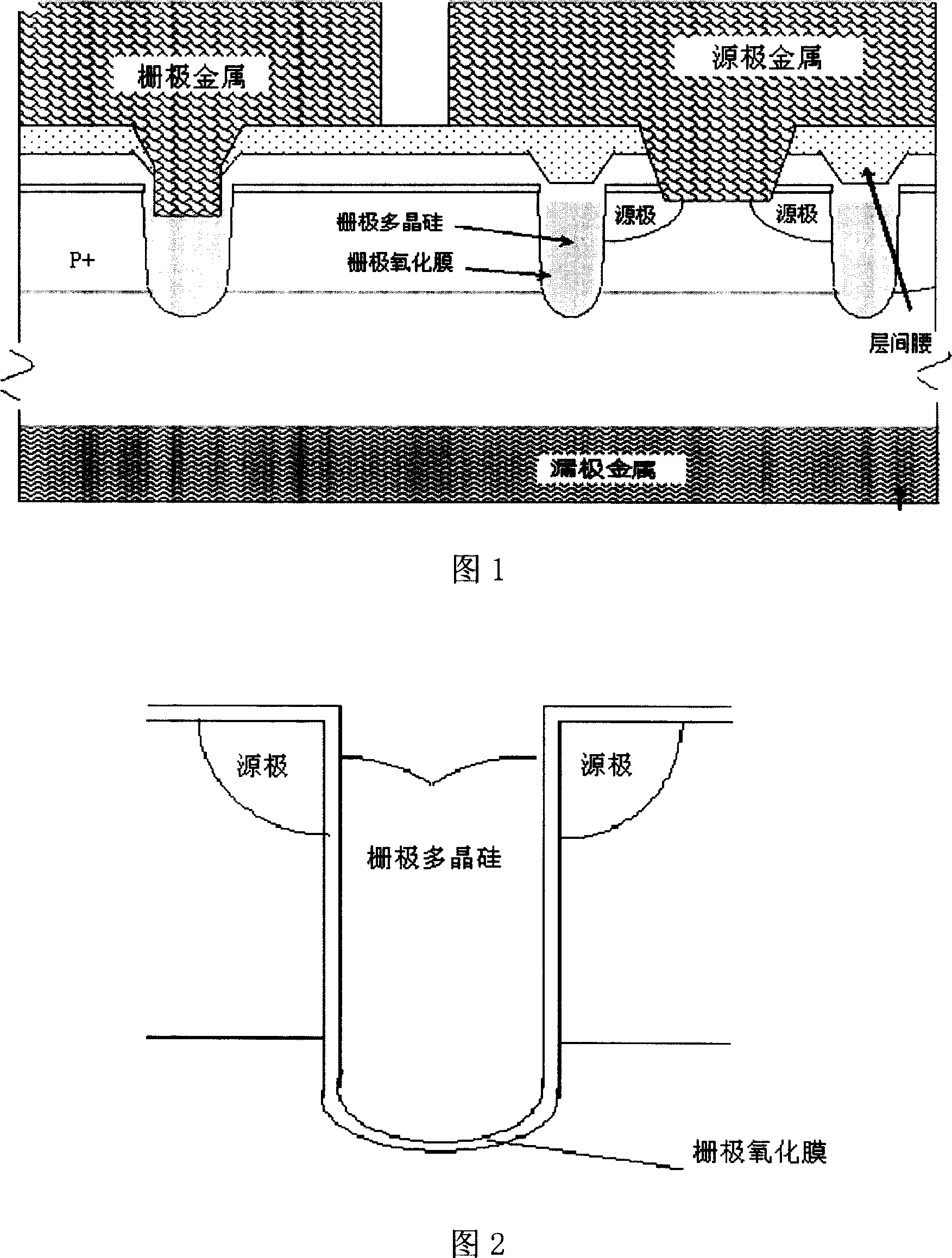
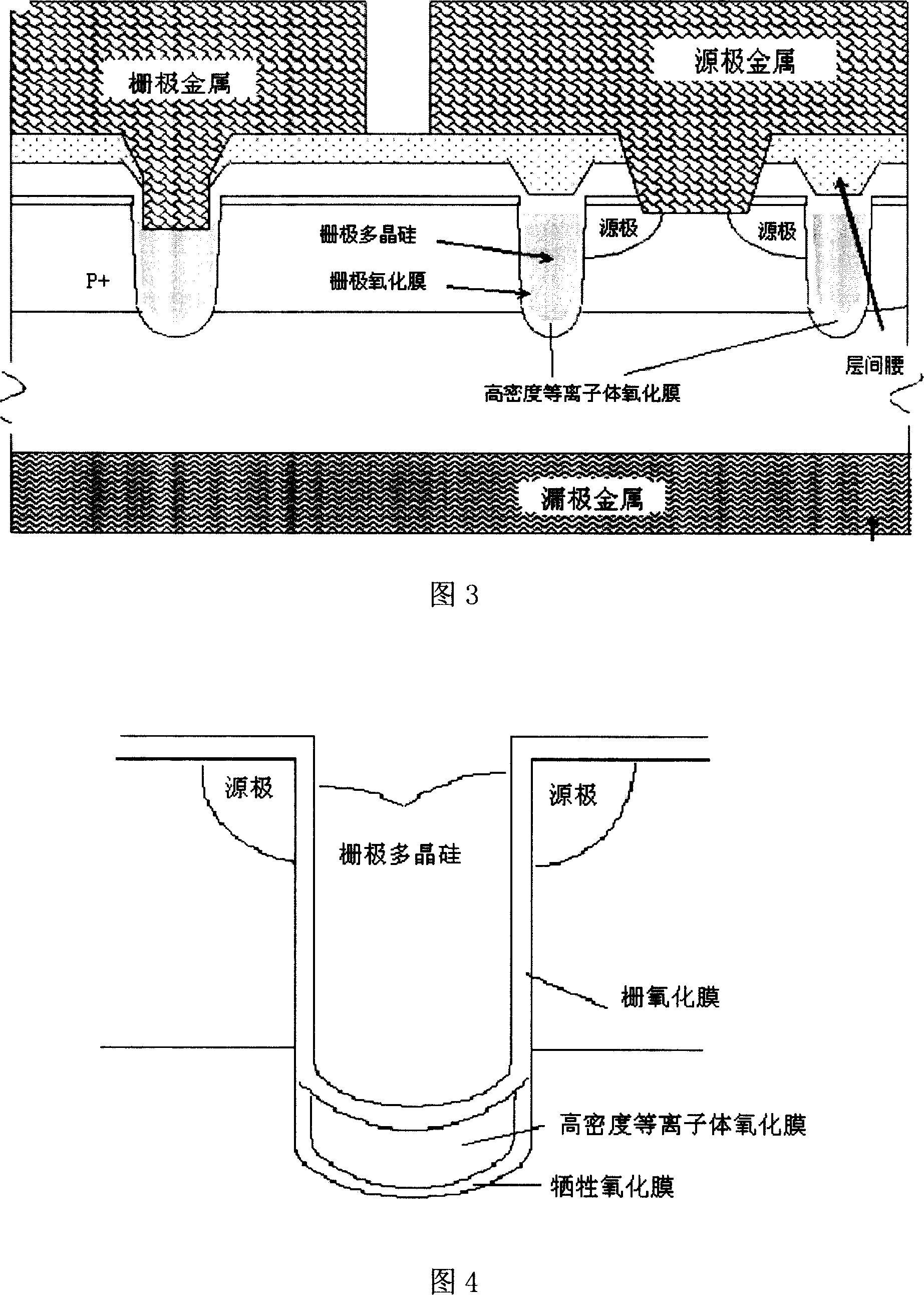
[0019] The method of the present invention includes the following steps:

[0020] (1) Deep trenches are formed by dry etching;

[0021] (2) On the bottom and sidewalls of the trench, a layer of sacrificial oxide film is grown, and the thickness of the sacrificial oxide film is about 300-500 angstroms;

[0022] (3) At the bottom and sidewalls of the trench, that is, on the top of the sacrificial oxide film grown in step (2), use high-density plasma deposition (HDP) to grow another layer with a thickness of 1000-3000 angstroms High-density plasma oxide film;

[0023] (4) Use a chemical solution, such as hydrofluoric acid, to remove the oxide film grown on the sidewall of the trench. The removed oxide film includes a sacrificial oxide film and a high-density plasma oxide film;

[0024] (5) At the positions of the sidewalls and the bottom of the trench, another layer of gate oxide film is grown;

[0025] (6) Growing and engraving the gate polysilicon in the trench;

[0026] Following ...


PUM

PropertyMeasurementUnit
Thicknessaaaaaaaaaa
Thicknessaaaaaaaaaa

Abstract

The invention discloses a manufacturing method of trench-MOS transistor, aiming at lowering the capacitor between the gate and drain, and increase switching rate of transistor. This method includes the following steps: use dry etching to form a deep trench; grow a layer of sacrificial oxide film; then continue to use the technique of high-density plasma deposition to grow a layer of high-density growth of the plasma membrane in the bottom and the wall of mentioned trench; and then use certain liquid to remove the oxide film on the surface of mentioned trench. That removal of oxide film contains sacrificial oxide film and high-density Plasma oxide film; then continues to grow a layer of the gate oxide film in the bottom and on the wall of the mentioned trench wall; then perform the growth and carve of polysilicon within the trench.

Description

technical field [0001] The invention relates to a manufacturing method of a semiconductor device, in particular to a manufacturing method of a trench type MOS transistor capable of reducing bottom capacitance. Background technique [0002] In power devices, switching characteristics have gradually become a main parameter to measure the performance of these devices, and to improve their switching characteristics must reduce their overall capacitance. At present, the manufacturing method of trench MOS transistors is generally as follows: (1) forming a deep trench by dry etching; (2) growing a sacrificial oxide film through a diffusion furnace; (3) removing the sacrificial oxide film; (4) Growth of gate oxide film; (5) growth of gate polysilicon; (6) etching back gate polysilicon below the silicon plane; (7) lithography implantation of base region and source region; (8) growth of interlayer film and contact hole formation; (9) front metal sputtering and etching; (10) back thin...

Claims


Application Information

Patent Timeline
IPC IPC(8): H01L21/336
Inventor 张朝阳姜宁李建文
Owner SHANGHAI HUAHONG GRACE SEMICON MFG CORP
Why Eureka
Try Eureka