


Quick Research
Generate reliable direction feasibility study reports for your R&D in just a few steps.

Technical Q&A
Discover and master advanced knowledge NOW. Basics, ideas, possibilities, all at once.

Find Solutions
As an expert in R&D theories, this can generate solutions to your technical problems instantly.

Evaluate Feasibility
Analyze your overall solution with one click, know your potential R&D risks in advance.

Monitor Landscape
Get weekly tech updates, stay abreast of the latest tech innovations and key insights.
Method of growing gallium nitride crystal
A gallium nitride and crystal technology, which is applied in the field of manufacturing high-quality gallium nitride substrates, can solve the problems of undisclosed and constant formation of polarity inversion regions, etc.
- Summary
- Abstract
- Description
- Claims
- Application Information
AI Technical Summary
Problems solved by technology
Method used
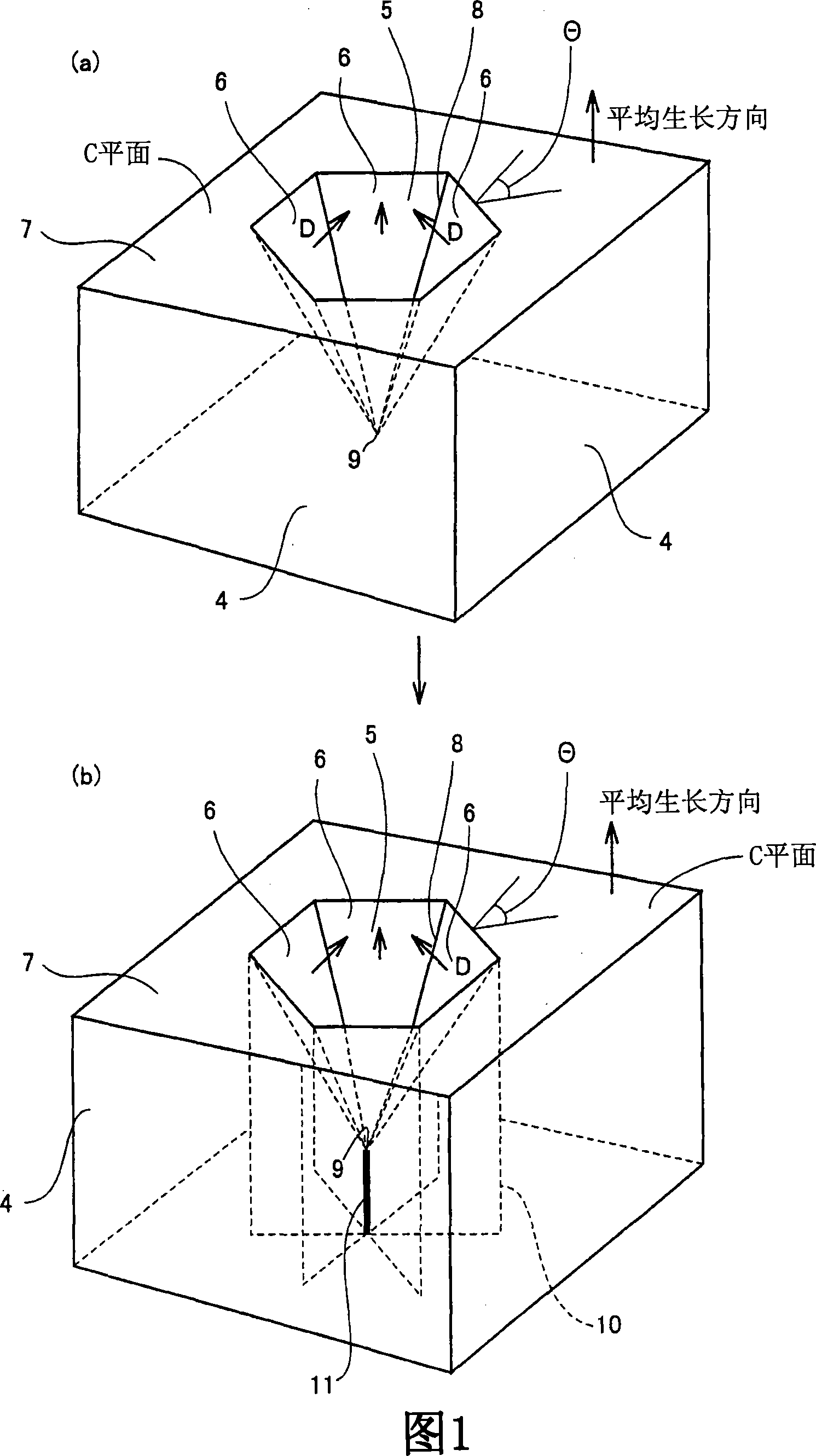
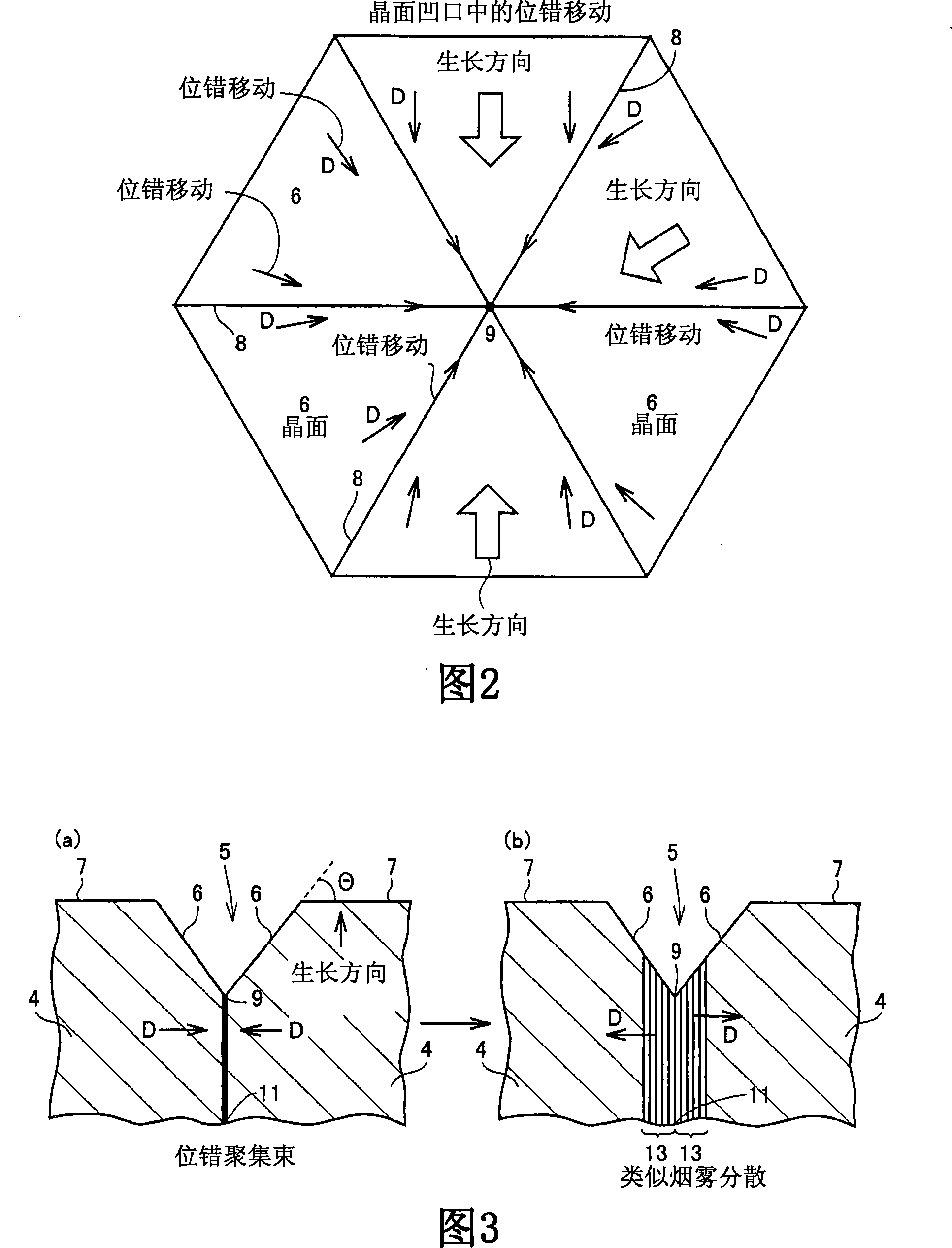
Image

Examples
example 1
[0111] Example 1 (the degree of formation of the polarity reversal region J caused by the first growth temperature Tj)
[0112] 1. Base substrate (U)
[0113] A 2-inch diameter sapphire substrate (U1), a GaAs substrate (U2), and a sapphire substrate (U3) (on which a 1.5 μm thick GaN epitaxial layer was formed by the MOCVD method) were prepared as base substrates. The sapphire substrate (U1) is a substrate whose C plane ((0001) plane) is the main surface. The GaAs substrate (U2) is a substrate having a (111)A plane (ie, Ga plane) as a main surface. The GaN / sapphire substrate (U3) is a mirror-like substrate in which an epitaxial layer of a GaN layer is formed on the C plane ((0001) plane) of the sapphire substrate. This substrate equipped with an epitaxial layer is also called a template.
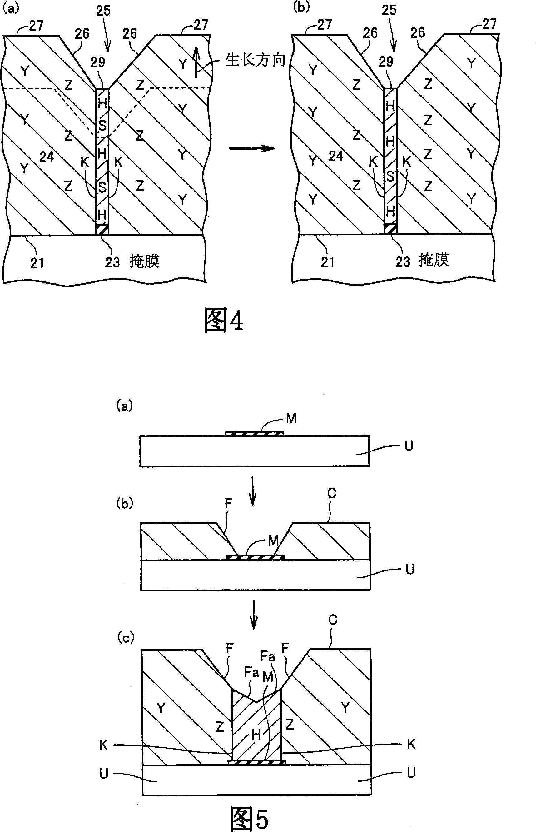
[0114] 2. Mask pattern (M)
[0115] On each of the three types of base substrates U1, U2, and U3, a 1μm thick SiO is formed by the plasma CVD (chemical vapor deposition) method 2 film. Through ph...
example 2
[0181] Example 2 (Difference caused by growth rate Vj)
[0182] Use the same reactor as in Example 1 and change the growth rate, as in Example 1, when equipped with SiO 2 On the GaAs (111) substrate (U2) of the strip type mask (M1) and the dot type mask (M2), gallium nitride crystals are grown. The relationship between the crystal growth rate Vj of the gallium nitride crystal and the ease of formation of the polarity inversion region J was examined.
[0183] In the HVPE reactor, the above-described substrate with a mask (two types of substrates, of which one type of base substrate U2 is equipped with two types of mask patterns M1 and M2) is placed. Initially, at a low temperature of about 500°C (Tb=500°C (773.15K)), the partial pressure of NH3 gas P NH3 =0.2atm(20kPa), and the partial pressure of HCl gas P HCl = 2×10 -3 Atm (0.2kPa) and a growth time of 15 minutes, a buffer layer of GaN is formed. The thickness of the buffer layer is 60 nm.
[0184] Subsequently, the temperature i...
example 3
[0225] Example 3 (The difference caused by the growth rate Vj at different growth temperatures)
[0226] The present inventors repeatedly conducted experiments as described in Examples 1 and 2, and found that the ease of formation of the polarity inversion region depends on the crystal growth temperature and the crystal growth rate at the crystal growth temperature. In the following example 3 and the following examples, the ease of formation of the polarity inversion region J is checked by the growth rate Vj at a growth temperature different from that of the example 2.
[0227] Using the same reactor as in Example 1, at a growth temperature different from that in Example 2, and changing the growth rate, the strip type mask (M1) and dot type mask (M1) equipped with SiO2 as in Examples 1 and 2 M2) GaAs (111) substrate (U2), grow gallium nitride crystal. The relationship between the crystal growth rate Vj of the gallium nitride crystal and the ease of formation of the polarity invers...
PUM
| Property | Measurement | Unit |
|---|---|---|
| thickness | aaaaa | aaaaa |
| thickness | aaaaa | aaaaa |
| thickness | aaaaa | aaaaa |
Abstract
Description
Claims
Application Information
 - R&D Engineer
- R&D Manager
- IP Professional
- Industry Leading Data Capabilities
- Powerful AI technology
- Patent DNA Extraction
Browse by: Latest US Patents, China's latest patents, Technical Efficacy Thesaurus, Application Domain, Technology Topic, Popular Technical Reports.
© 2024 PatSnap. All rights reserved.Legal|Privacy policy|Modern Slavery Act Transparency Statement|Sitemap|About US| Contact US: help@patsnap.com