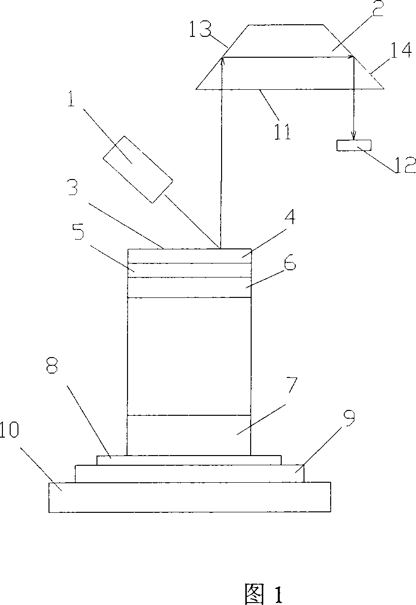
A vertical outside cavity radiation semiconductor laser
A technology of semiconductors and lasers, applied in the field of vertical external cavity surface emitting semiconductor lasers, which can solve the problems of long debugging time and lack of mechanical and thermal stability of lasers, and achieve simple structure, good mechanical and thermal stability, and position adjustment simple effect
- Summary
- Abstract
- Description
- Claims
- Application Information
AI Technical Summary
Problems solved by technology
Method used
Image
Examples
Embodiment 1
[0012] For the output light with a lasing wavelength of 980nm, the pump light source 1 is a high-power semiconductor laser array with a wavelength of 800-810nm, the Paul prism is made of BAK4 or BAK7, the antireflection film 3 is Ta205, the window layer 4 is InGaP or AlGaAs, and the light absorption Layer 5 is AlGaAs, periodic multi-quantum well active gain region 6 is In0.16Ga0.84As quantum well and Ga0.06As0.94P potential barrier, semiconductor distributed Bragg reflector 7 is 25-30 pairs of AlGaAs / GaAs, and the solder is indium , the heat sink 8 is diamond or Si, the heat sink 9 is copper or oxygen-free copper or pure copper, the heat-conducting adhesive is heat-conducting silicon, the microchannel heat sink 10 is copper or oxygen-free copper or Si material, and the output coupling mirror 12 is an optical Glass. In this way, a 980nm optically pumped vertical external-cavity surface-emitting semiconductor laser with a coupling cavity formed by a Paul prism can be obtained. ...
Embodiment 2
[0014] The pumping light source 1 among the embodiment 1 is replaced by a high-power 630-670nm semiconductor laser array, and the periodic multi-quantum well active gain region 6 is replaced by a GaAs quantum well and an A10.2Ga0.8As potential barrier, so that it can be obtained by The 850nm optically pumped vertical external-cavity surface-emitting semiconductor laser constituted by the Paul prism is coupled to the cavity.
Embodiment 3
[0016] The pumping light source 1 in embodiment 1 is replaced by a 975-1250nm high-power semiconductor laser array, the window layer 4 is replaced by InP, the periodic multi-quantum well active gain region 6 is replaced by InGaAsP / InP, and the semiconductor distributed Bragg reflector 7 Replace it with 25-30 pairs of InP / InGaAsP, so that a 1150nm optically pumped vertical external cavity surface emitting semiconductor laser with a coupling cavity formed by a Paul prism can be obtained.
PUM
 Abstract
Description
Claims
Application Information
