Electric pump micro cavity laser with integrated straight wave guide output

A straight waveguide and laser technology, applied in the field of optoelectronics, can solve the problems of complex process, high precision requirements, and difficult directional output of optical power, and achieve the effect of high output coupling efficiency and simple structure

Inactive Publication Date: 2008-03-26
CHANGCHUN INST OF OPTICS FINE MECHANICS & PHYSICS CHINESE ACAD OF SCI
View PDF0 Cites 14 Cited by
  • Summary
  • Abstract
  • Description
  • Claims
  • Application Information

AI Technical Summary

Problems solved by technology

[0005] In order to overcome the shortcomings of the prior art that the optical power is difficult to output in a directional manner, and to solve the problems of high precision requirements and complex processes of U-shaped structured light pumped microcavity lasers, the present invention discloses an electrically pumped microcavity with integrated output straight waveguide Laser, the laser in the microcavity laser can be output through the port of the integrated output straight waveguide. This device is a microcavity laser that generates laser oscillation based on the principle of whispering gallery mode

Method used


Image

  • Electric pump micro cavity laser with integrated straight wave guide output
  • Electric pump micro cavity laser with integrated straight wave guide output
  • Electric pump micro cavity laser with integrated straight wave guide output

Examples


Embodiment 1

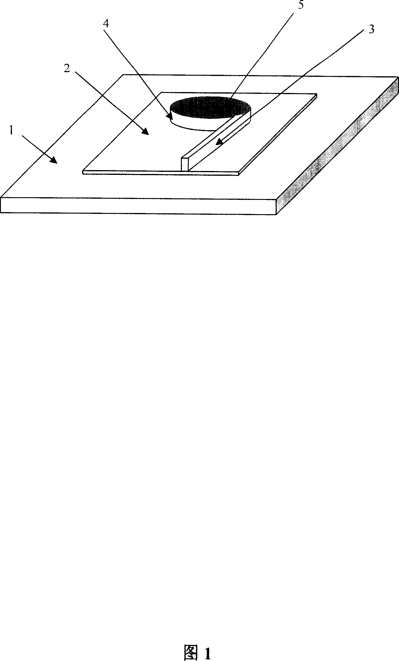
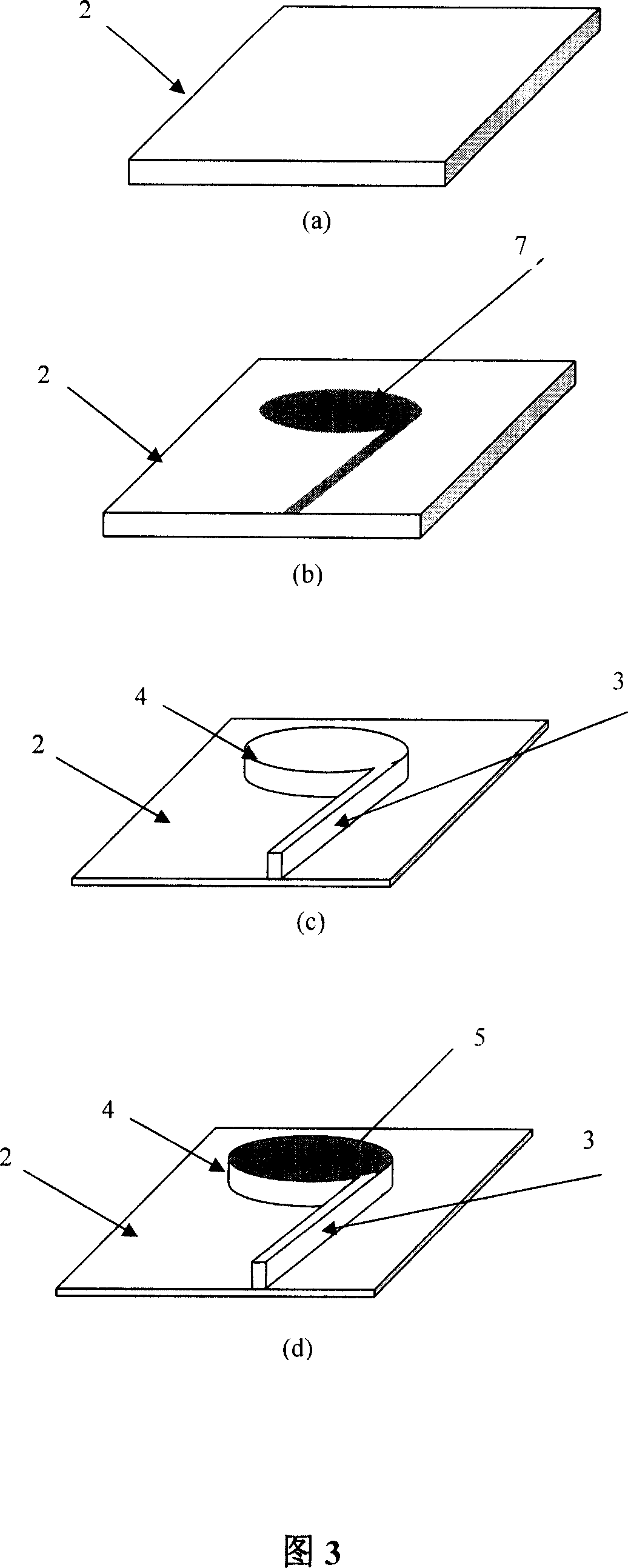
[0018] Fig. 3 is a schematic diagram of the preparation of an electrically pumped microcavity laser with a microdisk integrated output straight waveguide.

[0019] (1), figure (a) is the sample of the semiconductor quantum well laser material grown with MOCVD or MBE technology on the substrate (2), and the thickness of the quantum well laser material is 2-3 microns.

[0020] (2) According to the structural design of the microdisk and the output straight waveguide, a photolithography plate for photolithography is prepared. In this example, the diameter of the microdisk can be designed to be 50 microns, the width of the straight waveguide to be 5 microns, and the length to be 100 microns. Figure (b) uses a photolithographic method to transfer the pattern (7) of the laser to be prepared to the surface of the sample in Figure (a) with photoresist.

[0021] (3), Figure (c) is the sample of Figure (b) after the transfer of the laser pattern, using chemical etching to carve out the ...

Embodiment 2

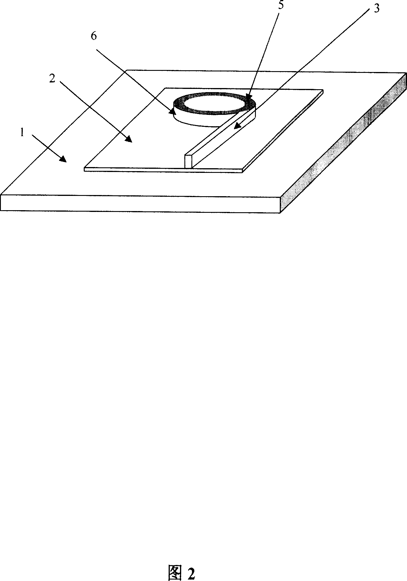
[0026] The manufacturing process of the electrically pumped microcavity laser with integrated output straight waveguide of the microring type shown in FIG. 2 is the same as that of Embodiment 1. The only difference is that the photoresist plate required for pattern transfer in Figure 3(b) is replaced with a photoresist plate prepared according to the structure design of the microring and the output straight waveguide. In this example, the outer diameter of the microring can be designed to be 50 microns, the inner diameter to be 30 microns, and the width of the straight waveguide to be 5 microns and the length to be 100 microns.


PUM


Abstract

This invention discloses an electric pump micro-cavity laser outputting laser from a port of an integrated straight waveguide based on a whisper cloister mode theory and composed of a die and heat sink, in which, the die is a chip processed in complecated processes of photoetch, corrosion, oxidation and evaporation of electronic beams on the epitaxial chip of a semiconductor quantum well laser, and the center of which is a micro-disk or a micro-loop, a straight waveguide of several mum wide, several decades-several hundreds long and same thick to the disk or the loop is integrated along the tangent of the edge of the disk or loop, in which, an ohmic contact metal film is prepared on the surface of the disk or the loop and a sloder is applied to weld the die and the heat sink.

Description

[0001] Technical field: The present invention belongs to the field of optoelectronic technology, and is an electrically pumped microcavity laser for all-optical integration. Background technique: [0002] Semiconductor whispering gallery mode microcavity lasers have the advantages of small size, low lasing threshold, and high integration. Whispering corridor mode laser propagates in the direction parallel to the surface of the device inside the device, and can realize on-chip interconnection and integration with optical detectors and optical couplers to meet the needs of large-scale integrated optical circuits. key components. [0003] The basic structure of whispering corridor mode microcavity laser reported at home and abroad is microdisk or microring. Relying on the refractive index difference between the edge of the micro-disk or the micro-annular micro-cavity and the air, the light propagating in it forms total reflection. Through this total reflection, oscillation can ...

Claims


Application Information

Patent Timeline
Patent Type & Authority Applications(China)
IPC IPC(8): H01S5/00
Inventor 宁永强秦莉孙艳芳李特崔锦江刘云刘星元王立军
Owner CHANGCHUN INST OF OPTICS FINE MECHANICS & PHYSICS CHINESE ACAD OF SCI
Why Eureka
Try Eureka