Apparatus for manufacturing semiconductor device, wet etching process device and wet etching process method

A technology of etching treatment and manufacturing method, which is applied in the direction of semiconductor/solid-state device manufacturing, manufacturing microstructure devices, microstructure devices, etc., which can solve the problems of undercutting increase and achieve the effect of reducing undercutting and inhibiting fracture

Inactive Publication Date: 2008-04-02
OKI ELECTRIC IND CO LTD
View PDF6 Cites 4 Cited by
  • Summary
  • Abstract
  • Description
  • Claims
  • Application Information

AI Technical Summary

Problems solved by technology

[0010] In the case of MEMS products with a thicker etched layer, etc., the problem of increased undercutting becomes significant when the immersion time in the etching solution increases

Method used


Image

  • Apparatus for manufacturing semiconductor device, wet etching process device and wet etching process method
  • Apparatus for manufacturing semiconductor device, wet etching process device and wet etching process method
  • Apparatus for manufacturing semiconductor device, wet etching process device and wet etching process method

Examples


Embodiment Construction

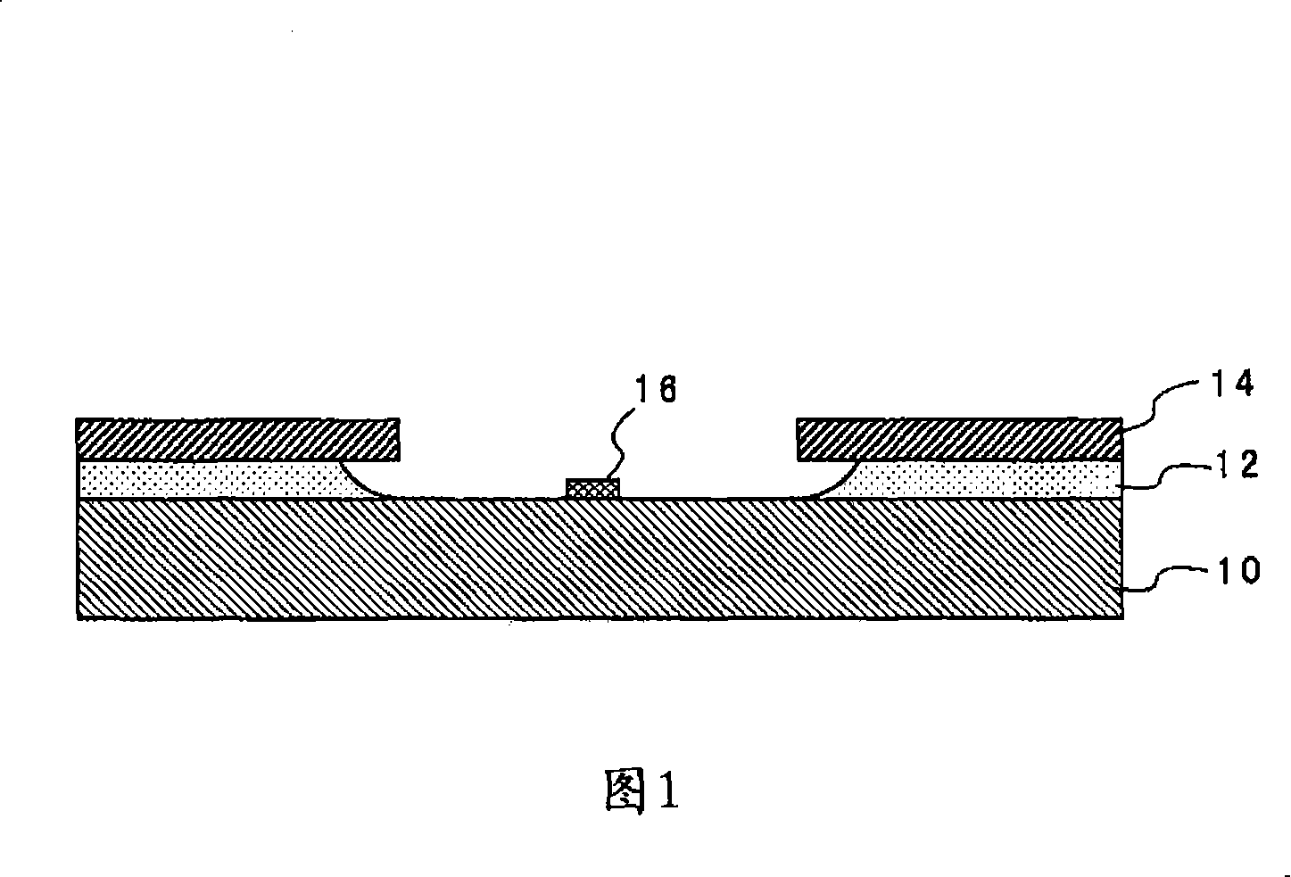
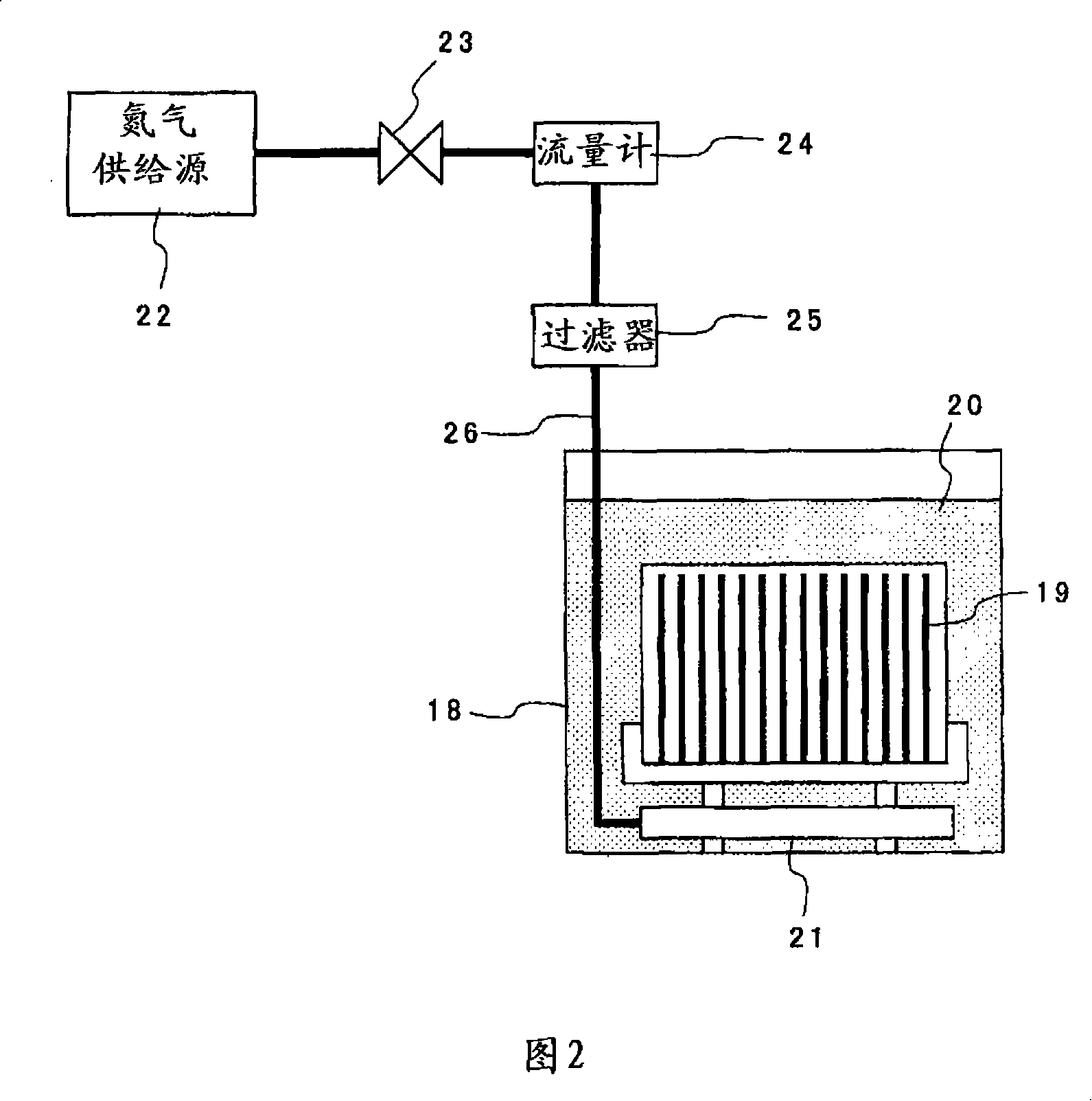
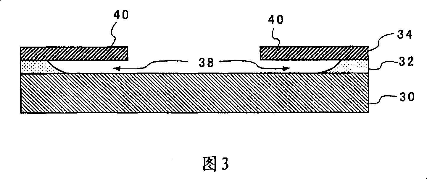
[0029] Hereinafter, the best mode for carrying out the invention will be described in detail with reference to FIGS. 4 to 7 . 4 is an explanatory diagram showing a schematic configuration of a wet etching apparatus according to an embodiment of the present invention. The wet etching apparatus according to this embodiment has an etching solution tank 118 that stores an etching solution 118 and performs wet etching on a plurality of semiconductor wafers 119 to be processed. As the etching solution (etchant) 120, a mixed chemical solution of hydrofluoric acid, ammonium fluoride, and acetic acid can be used. Wet etching can be used for the etching of the interlayer insulating film, nitride film, and oxide film after the metal wiring process.

[0030] Near the bottom of the etching solution tank 118, below the semiconductor wafer 119, a bubbler 121 for making nitrogen gas into fine bubbles is arranged.

[0031] The wet etching apparatus according to this embodiment further includ...


PUM


Abstract

An apparatus according to the present invention, includes an etching solution tank which contains etching solution used for a wet etching process, a wet etching process to a semiconductor wafer being carried out in the etching solution tank; a nitrogen gas supply component which supplies a nitrogen gas (N2), which is used for a wet etching process in the etching solution tank; a flow regulating component which delivers the nitrogen gas (N2) supplied from said nitrogen gas supply component into said etching solution tank during a wet etching process, and which continues to deliver said nitrogen gas into said etching solution tank during a standby phase in which a wet etching process is not being performed; and a bubbling component which bubbles said nitrogen gas (N2), supplied from said nitrogen gas supply component, in said etching solution tank during a wet etching process.

Description

technical field [0001] The present invention relates to a method of manufacturing a semiconductor device including a wet etching process. In particular, it relates to an improved method for controlling the foaming of nitrogen in etching solutions. Background technique [0002] The wet etching process, which is one of the manufacturing steps of semiconductor devices, is used to open holes in interlayer insulating films, open holes in PV films, and the like. In such a wet etching process, ammonium fluoride, the main component of the chemical solution (etching solution), tends to precipitate crystals, and because the precipitates float in the chemical solution, they sometimes adhere to the film to be etched on the surface of the wafer during immersion and hinder the process. Etching is performed. FIG. 1 shows how ammonium fluoride crystal precipitates 16 adhere to a film to be etched 12 on the surface of a wafer 10 . In addition, in FIG. 1 , reference numeral 14 denotes a re...

Claims


Application Information

Patent Timeline
Patent Type & Authority Applications(China)
IPC IPC(8): H01L21/306B81C1/00
CPCH01L21/67086H01L21/31111
Inventor 吉野和盛
Owner OKI ELECTRIC IND CO LTD
Why Eureka
Try Eureka