Non-volatile semiconductor memory and manufacturing method thereof

A non-volatile, manufacturing method technology, applied in semiconductor/solid-state device manufacturing, semiconductor devices, electric solid-state devices, etc., to achieve the effect of shortening the erasing and writing time, less electrons, and low current density

Active Publication Date: 2008-04-02
SEMICON MFG INT (SHANGHAI) CORP +1
View PDF1 Cites 2 Cited by
  • Summary
  • Abstract
  • Description
  • Claims
  • Application Information

AI Technical Summary

Problems solved by technology

[0006] The problem solved by the present invention is to provide a non-volatile semiconductor memory and its manufacturing method for the defect that the data storage capacity of the non-volatile semiconductor memory in the prior art cannot meet the needs of technological development. single electron storage, and the density of nano-single-crystal silicon ions in the nano-single-crystal silicon floating gate can be adjusted by adjusting the formation process

Method used


Image

  • Non-volatile semiconductor memory and manufacturing method thereof
  • Non-volatile semiconductor memory and manufacturing method thereof
  • Non-volatile semiconductor memory and manufacturing method thereof

Examples


Embodiment Construction

[0026] The specific embodiments of the present invention will be described in detail below in conjunction with the accompanying drawings.

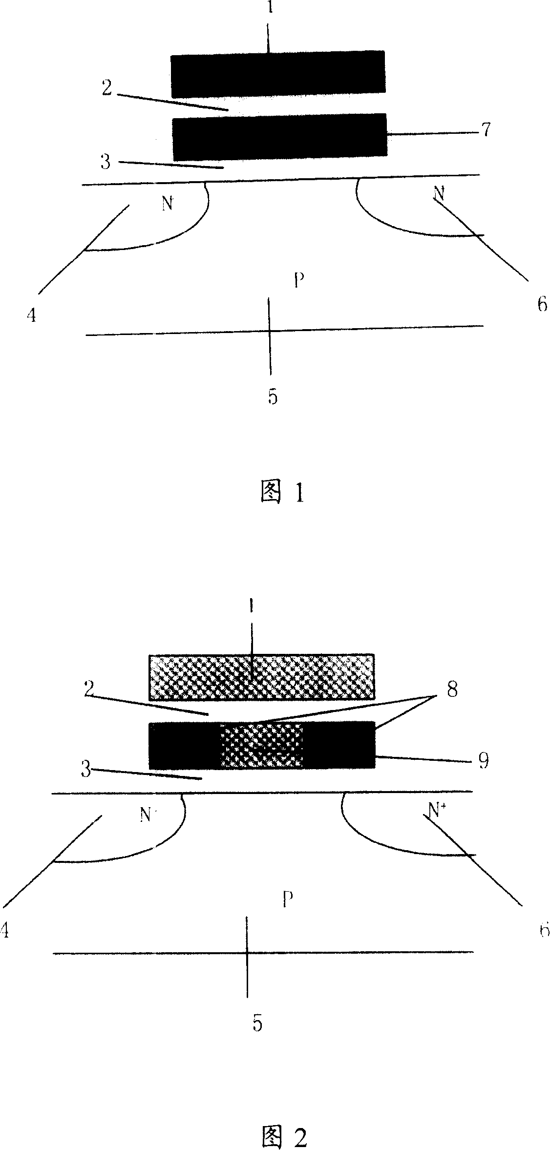
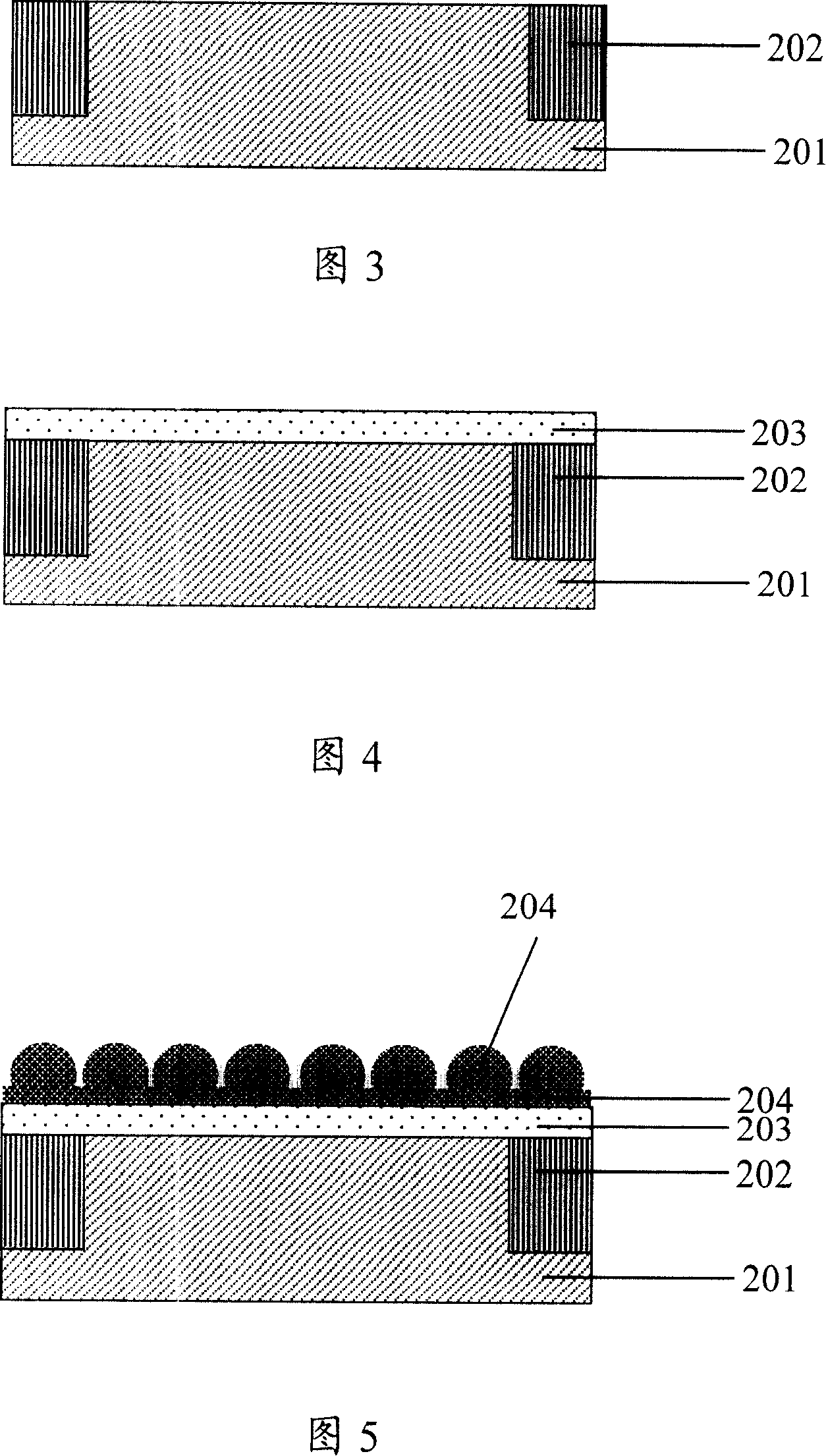
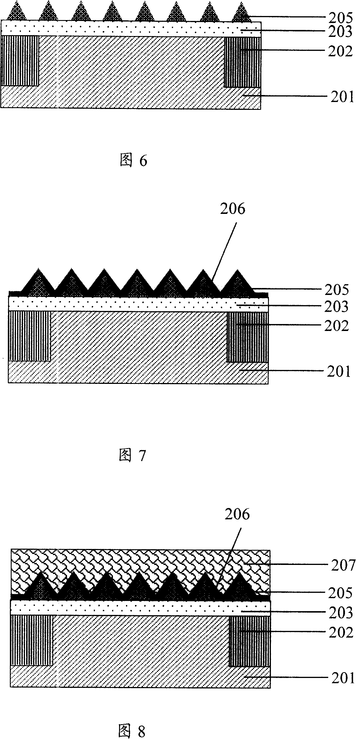
[0027] The invention provides a method for manufacturing a non-volatile semiconductor memory, comprising the following steps: forming a tunnel oxide layer on a semiconductor substrate; forming a nanometer single-crystal silicon layer on the tunnel oxide layer, and the nanometer single-crystal silicon layer is hillock-shaped Nano single crystal silicon particles; form an interlayer dielectric layer covering the nano single crystal silicon layer; form a polysilicon layer on the interlayer dielectric layer; pattern the polysilicon layer to form a control gate; pattern the interlayer dielectric layer to form blocking oxide layer; patterning the nano single crystal silicon layer to form a floating gate; doping the semiconductor substrate to form a separate source and drain; patterning the tunnel oxide layer to form a gate oxide layer, the contro...


PUM


Abstract

The present invention provides a non-volatile semiconductor memory and the manufacturing method thereof. The non-volatile semiconductor memory adopts a nanometer single crystal silicon floating gate to realize single-electron storage, and nanometer single crystal silicon ion in the nanometer single crystal silicon floating gate is high in density and strong in storage capacity. The manufacturing method of the non-volatile semiconductor memory comprises that: a tunnel oxide layer is formed on a semiconductor matrix; a nanometer single crystal silicon layer is formed on the tunnel oxide layer; the nanometer single crystal silicon layer is formed by nanometer single crystal silicon particles in knoll shape; an interlayer dielectric layer covering the nanometer single crystal silicon layer is formed; a polysilicon layer is formed on the interlayer dielectric layer; the polysilicon layer is patterned to form a control grid; the interlayer dielectric layer is patterned to form a barrier oxide layer; the nanometer single crystal silicon layer is patterned to form a floating gate; the semiconductor basal plate is intermingled to form a separate source electrode and a drain electrode; the tunnel oxide layer is patterned to form a thin gate oxide.

Description

technical field [0001] The invention relates to a non-volatile semiconductor memory, in particular, the invention relates to a non-volatile semiconductor memory containing a nano single-crystal silicon floating gate and a manufacturing method thereof. Background technique [0002] Non-volatile memory such as erasable programmable read-only memory (electrically programmable read-only memory, EPROM), electrically erasable programmable read-only memory (electrically-erasable programmable read-only memory, EEPROM) and flash memory (flash memory) At present, it is widely used as a data storage device in computer systems, and it can still save data information when the system is turned off or there is no power supply. [0003] A non-volatile memory (NVM) is usually a MOS transistor, with a source, a drain, a control gate and a floating gate, the floating gate is isolated from other part. [0004] Traditional non-volatile memories use polysilicon floating gates. Taking flash memo...

Claims


Application Information

Patent Timeline
Patent Type & Authority Applications(China)
IPC IPC(8): H01L21/336H01L21/28H01L21/8247H01L29/788H01L29/423H01L29/49H01L27/115
Inventor 肖德元金钟雨陈国庆李若加
Owner SEMICON MFG INT (SHANGHAI) CORP
Why Eureka
Try Eureka