Wet oxidation preparation method of Cu2O resistor memory

A resistance memory, wet oxidation technology, applied in the field of microelectronics, achieves the effects of uniform storage medium, low cost and simple process

Inactive Publication Date: 2008-04-09
FUDAN UNIV
View PDF1 Cites 6 Cited by
  • Summary
  • Abstract
  • Description
  • Claims
  • Application Information

AI Technical Summary

Problems solved by technology

[0004] The object of the invention is to propose a Cu x The wet oxidation preparation method of O resistance memory and the integration method with the copper interconnection process to overcome the shortcomings of the above two existing preparation methods

Method used


Image

  • Wet oxidation preparation method of Cu2O resistor memory
  • Wet oxidation preparation method of Cu2O resistor memory
  • Wet oxidation preparation method of Cu2O resistor memory

Examples


Embodiment 1

[0068] Example 1, integration with dual damascene process.

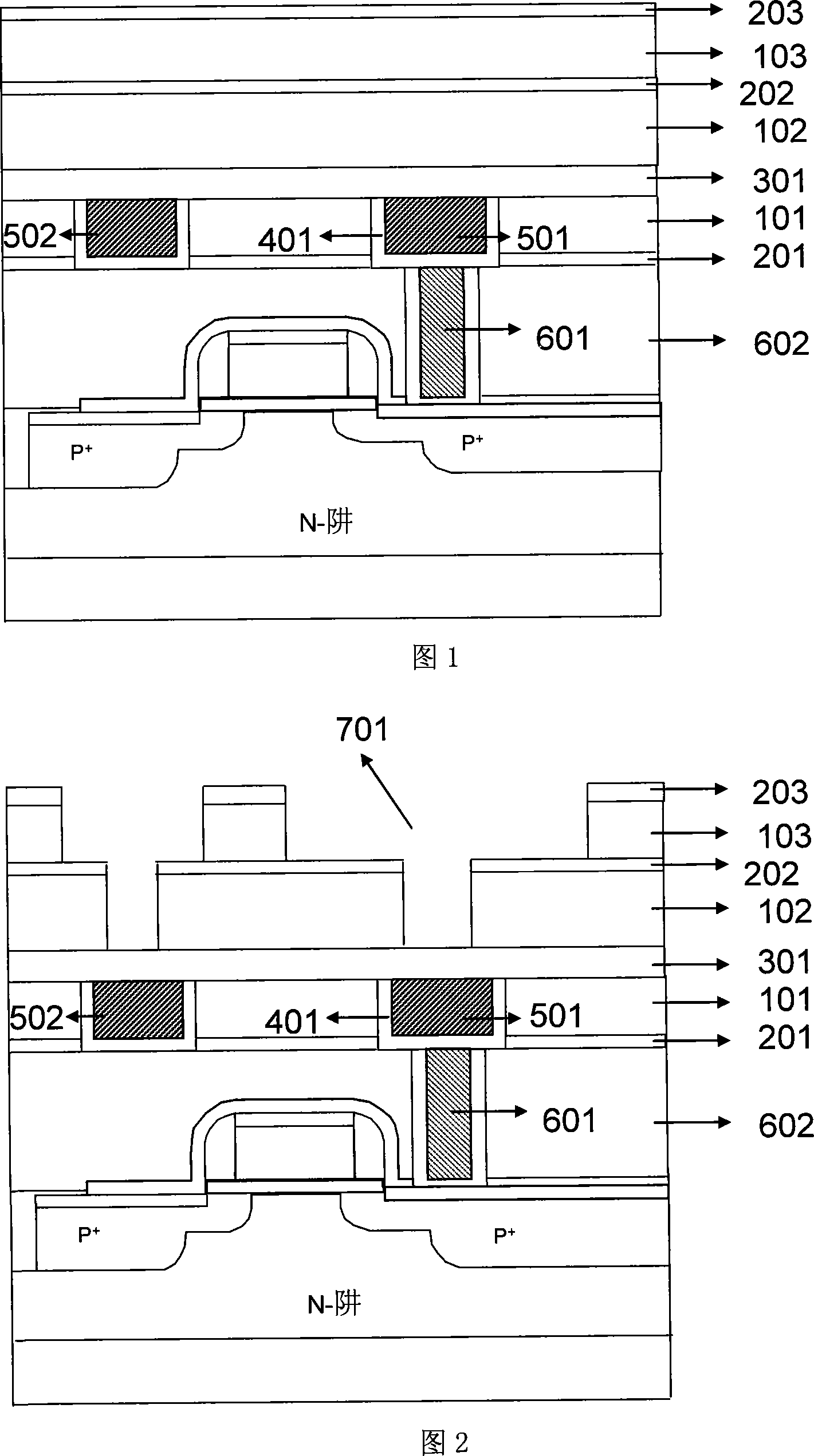
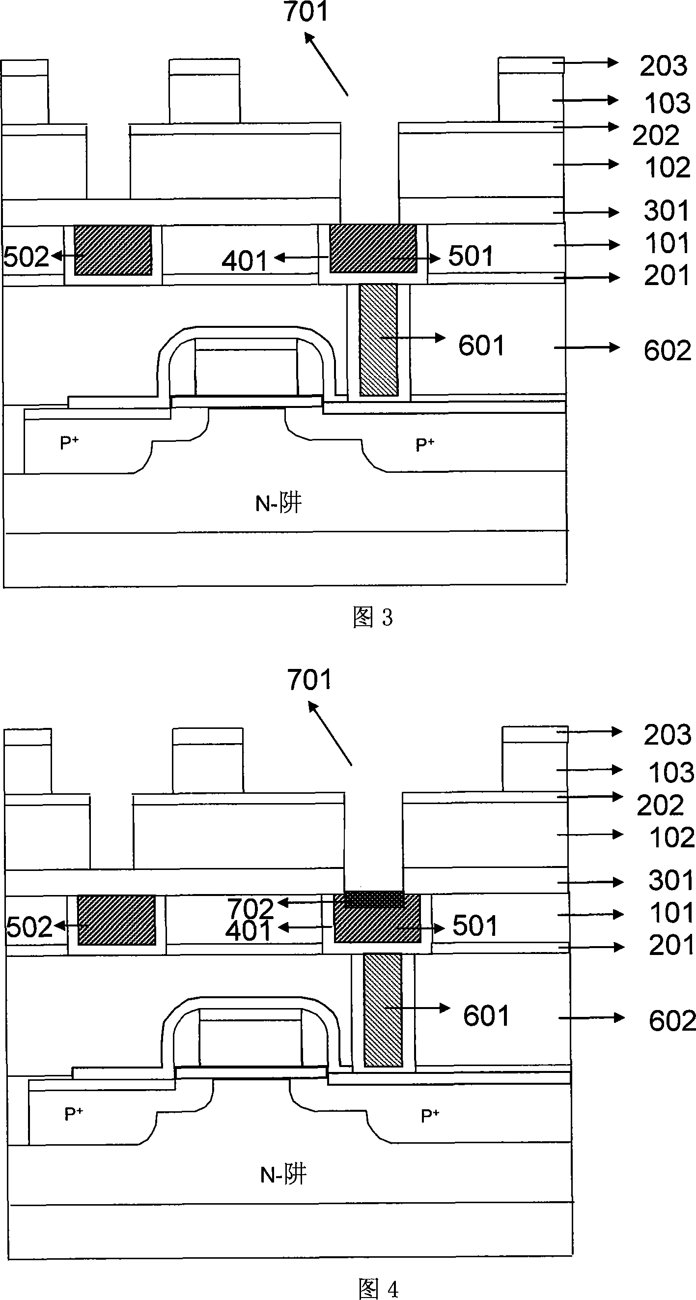
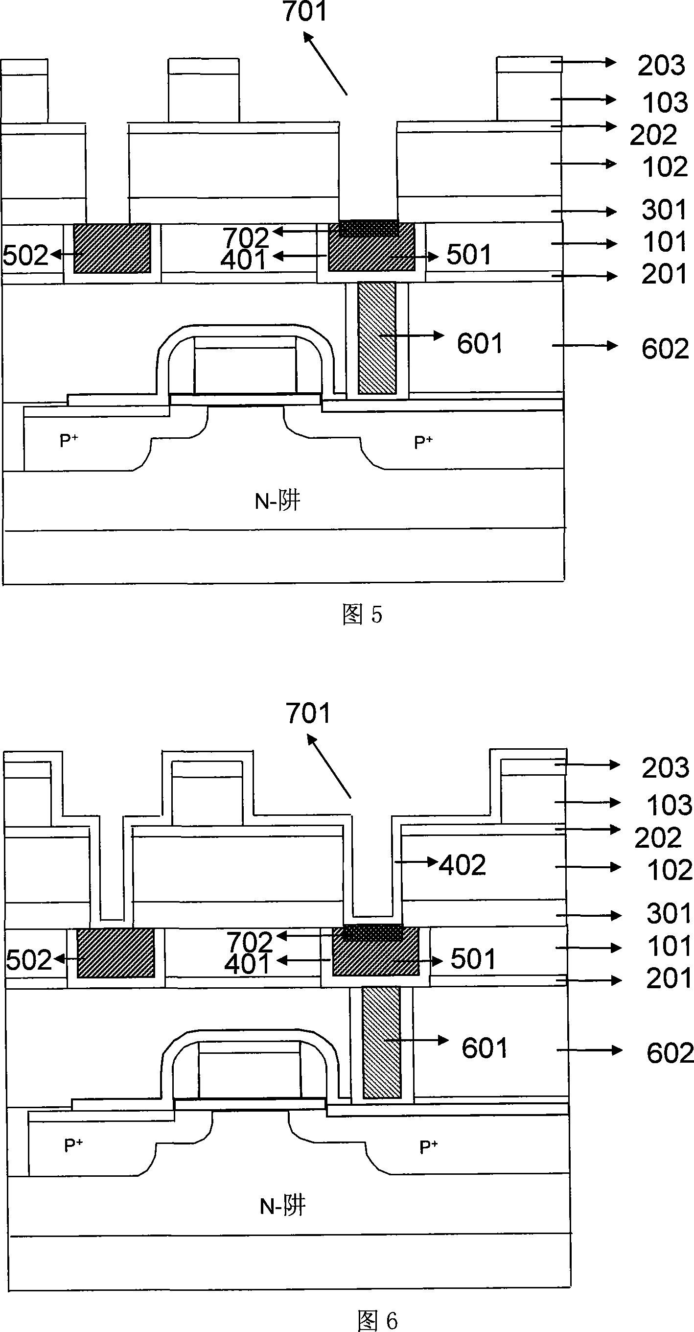
[0069] Figures 1 to 9 are cross-sectional views according to embodiments of the present invention. Figures 1 to 9 illustrate Cu x Process method of O resistance memory wet oxidation method integrated with double damascene copper interconnection process and formed between the first layer copper lead and the second layer lead, Cu x O is formed on the first layer of copper lines and under the copper plugs. However, the present invention is not limited to this embodiment.

[0070] Figure 1 is a cross-sectional view after the conventional double damascene copper interconnection process is completed until the first layer of copper wiring is fabricated, and the cap layer, interlayer dielectric (IMD) and etch stop layer are deposited. 602 is a PMD layer, which refers to the dielectric layer between the first layer of leads and the MOS device, and it can be a doped silicon oxide layer, such as silicon oxide doped with phosp...

Embodiment 2

[0091] Example 2, integration with a single damascene process.

[0092] Figures 10 to 20 are cross-sectional views according to Embodiment 2 of the present invention, and Figures 10 to 20 show Cu x The process method of O resistance memory wet oxidation method integrated with single damascene process and formed between the first layer copper wiring and the second layer wiring, Cu x O is formed under the second layer of copper lines and above the copper plugs. But the present invention is not limited to this embodiment.

[0093]FIG. 10 shows a cross-sectional view of a capping layer 301 and an interlayer dielectric (IMD) 102 after the conventional single damascene copper interconnection process is completed until the first layer of copper wiring is fabricated. 602 is the PMD layer, which refers to the dielectric layer between the first layer of wiring and the MOS device, which can be a dielectric material such as phosphorous-doped silicon oxide PSG; 601 is a tungsten plug, wh...

Embodiment 3

[0117] Embodiment 3 and above electrode are as the Cu of protective layer structure x O resistance memory manufacturing process integration

[0118] Figures 21 to 35 are cross-sectional views according to Embodiment 3 of the present invention. Figures 21 to 35 show Cu x Cu prepared by wet oxidation method for O resistance memory with the above electrode as protective layer structure x O-resistance memory manufacturing process is integrated and formed between the first layer of copper wiring and the second layer of wiring, Cu x O is formed on the first layer of copper leads and below the copper plugs. However, the present invention is not limited to this embodiment.

[0119] Figure 21 shows a cross-sectional view after the conventional double damascene copper interconnection process is completed and the first layer of copper leads is fabricated.

[0120] Figure 22 is a cross-sectional view of the capping layer before photolithography, and 301 is a capping layer (liner), whi...


PUM

PropertyMeasurementUnit
thicknessaaaaaaaaaa

Abstract

The invention pertains to the field of microelectronic technology, in particular to a wet oxidation fabrication method of a CuxO resistance memory and an integration method of copper interconnection technique. In the memory, CuxO acting as the memory medium is fabricated by a wet oxidation method. The detailed steps are that hydrogen peroxide aqueous with a certain concentration (10 percent to 50 percent) has a contact with the surface of the exposed Cu leads under a certain temperature (40 to 80 degree) to obtain the memory medium CuxO. The method in the invention has easy technique, low cost and no pollution, the memory medium formed is uniform, and no new impurity is introduced, with the ease to integrate with the copper interconnection technique of integrated circuit.

Description

technical field [0001] The invention belongs to the technical field of microelectronics, in particular to a Cu x A wet oxidation preparation method for an O-resistance memory, and an integration method with a copper interconnection process. Background technique [0002] Memory occupies an important position in the semiconductor market. Due to the continuous popularization of portable electronic devices, the share of non-volatile memory in the entire memory market is also increasing. Recently, non-volatile resistive switching memory devices (Resistive Switching Memory) have attracted high attention because of their high density, low cost, and the ability to break through the limitations of technological generation development. Resistive memory uses the characteristics of the resistance of the storage medium to reversibly switch between high resistance and low resistance under the action of electrical signals to store signals. There are many kinds of storage media, including ...

Claims


Application Information

Patent Timeline
Patent Type & Authority Applications(China)
IPC IPC(8): H01L45/00H01L21/82H01L21/768
Inventor 林殷茵傅秀峰陈邦明吕杭炳唐立尹明
Owner FUDAN UNIV
Why Eureka
Try Eureka