Making method for silicon germanium extension layer

A technology of silicon germanium epitaxy and manufacturing method, applied in semiconductor/solid-state device manufacturing, coating, metal material coating process and other directions, can solve the problems of pattern loading effect, low yield, small margin of silicon germanium epitaxial layer, etc. Fast growth, low impact, high yield effects

Inactive Publication Date: 2008-04-30
UNITED MICROELECTRONICS CORP
View PDF0 Cites 7 Cited by
  • Summary
  • Abstract
  • Description
  • Claims
  • Application Information

AI Technical Summary

Problems solved by technology

[0004] However, if the uniformity of the silicon germanium epitaxial layer is not good, it will cause the problem of pattern loading effect, which makes the subsequent process difficult to control and affects the yield of the process.
Furthermore, if the selective epitaxial growth process for the silicon germanium epitaxial layer is not properly controlled, it is easy to form the silicon germanium epitaxial layer at an unintended location (that is, the selection margin is small), or the growth rate of the silicon germanium epitaxial layer is slow and the yield is low. low level problem
What's more, it will destroy the insulating spacer interface of the metal oxide semiconductor transistor

Method used


Image

  • Making method for silicon germanium extension layer
  • Making method for silicon germanium extension layer
  • Making method for silicon germanium extension layer

Examples


no. 1 example

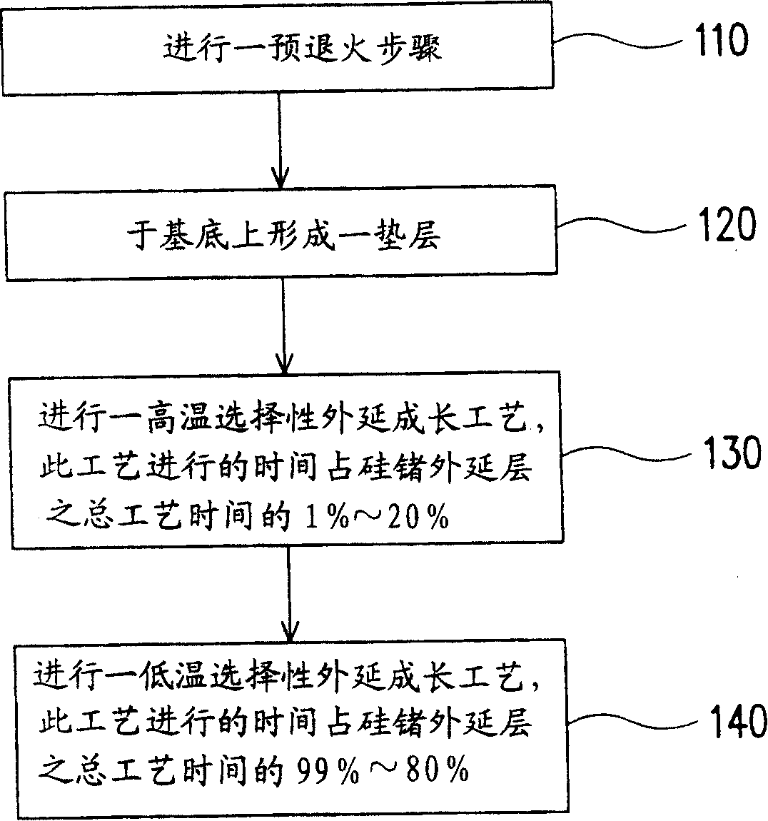
[0047] figure 1 It is a flow chart of manufacturing a silicon germanium epitaxial layer according to an embodiment of the present invention.

[0048] Please refer to figure 1 , a pre-annealing (pre-annealing) step 110 is performed first, and the temperature thereof is, for example, about 800° C. Then, a pad layer is formed on the substrate (step 120). The material of the underlayer is the same as that of the substrate, such as silicon.

[0049] Next, a high-temperature selective epitaxial growth process is performed, and the high-temperature selective epitaxial growth process takes 1% to 20% of the total process time of the SiGe epitaxial layer (step 130 ). In one embodiment, the time for the high temperature selective epitaxial growth process is, for example, 1%-15% of the total process time of the SiGe epitaxial layer, preferably 1%-10%, more preferably 3%-6%. In one embodiment, the high temperature selective epitaxial growth process is performed for about 30 seconds, fo...

no. 2 example

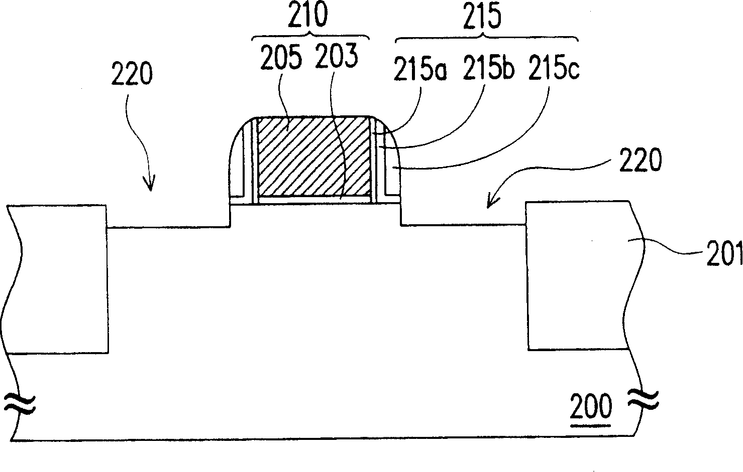
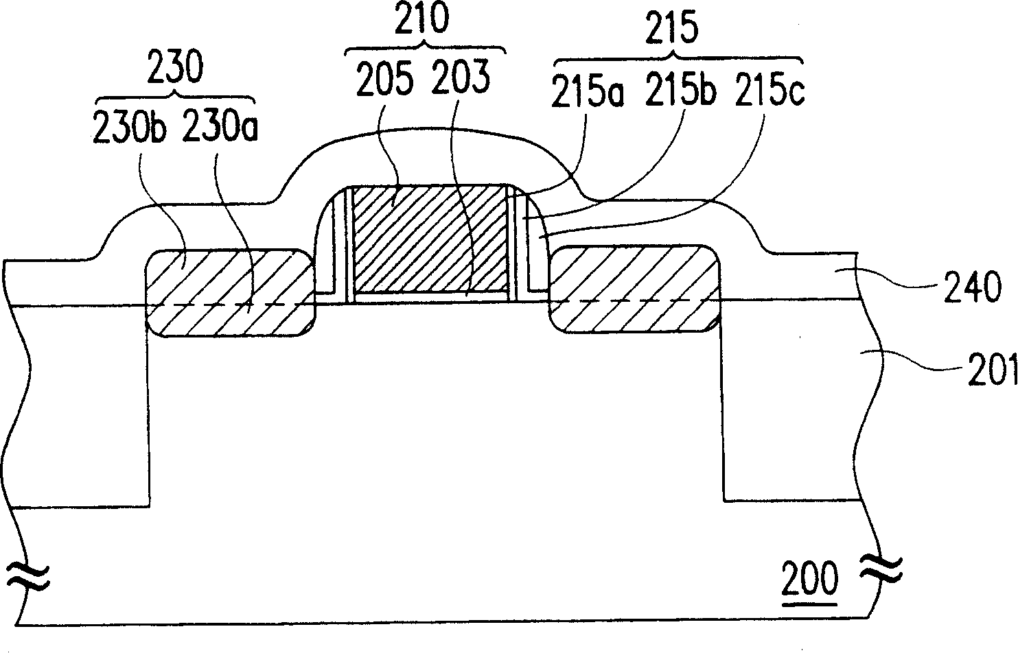
[0062] Figure 2A to Figure 2B It is a sectional view showing a manufacturing process of a silicon germanium epitaxial layer according to another embodiment of the present invention.

[0063] Please refer to Figure 2A Therefore, the method for manufacturing the silicon germanium epitaxial layer proposed by the present invention can be applied to the process of PMOS transistors. An isolation structure 201 is formed in the substrate 200 , and a gate structure 210 is formed on the substrate 200 . Wherein, the substrate 200 is, for example, a silicon substrate, and the isolation structure 201 is, for example, a silicon oxide shallow trench isolation structure. The gate structure 210 includes, for example, a gate dielectric layer 203 and a gate 205 from bottom to top. The material of the gate dielectric layer 203 is, for example, silicon oxide, and the material of the gate 205 is, for example, doped polysilicon, metal, metal silicide or other conductors. The SiGe epitaxial lay...

no. 3 example

[0084] Figure 4 It is a step diagram showing the manufacturing process of a silicon germanium epitaxial layer according to another embodiment of the present invention.

[0085] Please refer to Figure 4 In this embodiment, the silicon germanium epitaxial layer is, for example, formed on a substrate. The substrate is first subjected to a surface treatment step (step 410), such as pre-cleaning or gas diffusion. Then, a pre-annealing step (step 420 ), the temperature of the pre-annealing is, for example, about 800° C. is performed.

[0086] Next, a high-voltage selective process is performed, and the time for the high-voltage selective epitaxial growth process accounts for 1%-20% of the total process time of the SiGe epitaxial layer (step 430 ), preferably for example 8%-17%.

[0087] The pressure of the high-pressure selective epitaxial growth process is, for example, greater than or equal to 10 Torr (torr), and the temperature is, for example, 650°C. The reaction gas used ...


PUM


Abstract

The invention provides a method for manufacturing a silicon germanium epitaxial layer. The method includes: carrying out the first selective epitaxial growth process under the first condition, and the processing time accounts for 1%-20% of the total process time of the silicon germanium epitaxial layer. Then, a second selective epitaxial growth process is carried out under the second condition, and its processing time accounts for 99%-80% of the total processing time of the SiGe epitaxial layer. Wherein, the first condition and the second condition include temperature condition or pressure condition, and the reaction gases used in the first selective epitaxial growth process and the second selective growth process include at least silicon-containing gas and germanium-containing gas.

Description

technical field [0001] The invention relates to a method for forming a semiconductor structure, and in particular to a method for forming a silicon germanium epitaxial layer by a selective epitaxial growth process. Background technique [0002] When the semiconductor integrated circuit enters the deep sub-micron (Deep Sub-Micron) process, the size of the components is gradually reduced, so that the operating speed of the entire integrated circuit will be effectively improved. However, when the size of the device is further reduced, in the case of a metal oxide semiconductor transistor (MOS transistor), the resistance and parasitic capacitance of the gate and source / drain will increase accordingly, making the device smaller The resulting improvement of the overall circuit performance is hindered. If the device size continues to shrink, the area of ​​the entire device will be occupied by the source / drain ohmic contact (ohmic contact), thus setting the upper limit of the integ...

Claims


Application Information

Patent Timeline
Patent Type & Authority Applications(China)
IPC IPC(8): H01L21/205C23C16/00C23C16/54
Inventor 江日舜施泓林唐力原蒋天福范铭棋廖晋毅简金城
Owner UNITED MICROELECTRONICS CORP
Why Eureka
Try Eureka