

Mask etch process
A technology of mask plate and mask layer, which is applied in the photoplate making process of patterned surface, photosensitive material processing, instruments, etc.
- Summary
- Abstract
- Description
- Claims
- Application Information
AI Technical Summary
Problems solved by technology
Method used
Image

Examples
Embodiment
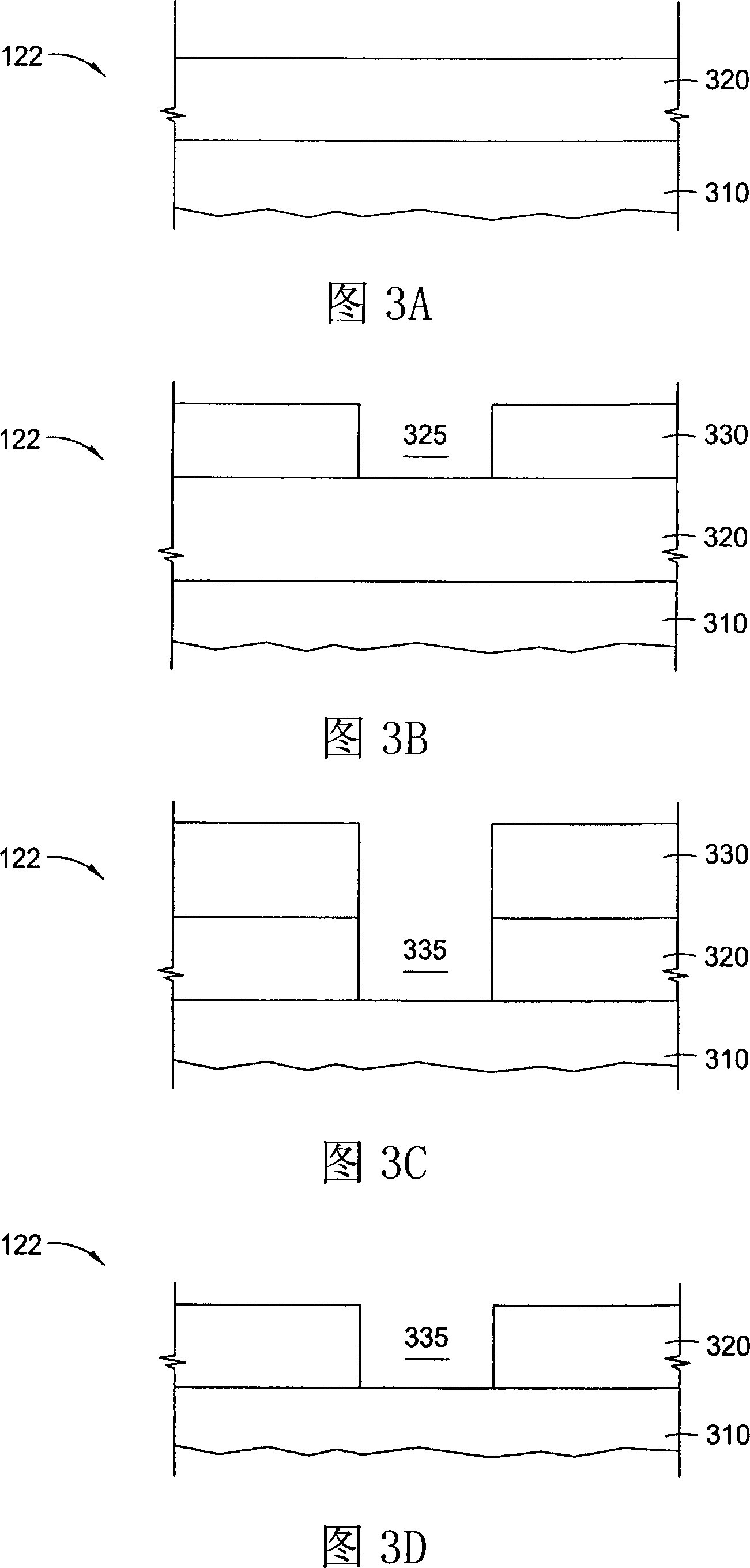
[0071] A photolithographic mask including a substrate formed of a light transmissive material such as optical quality quartz, fused silicon material, molybdenum silicide is introduced into a processing chamber for resist deposition (MoSi), molybdenum silicon oxynitride (MoSi X N Y o Z ), calcium fluoride, alumina, sapphire, or combinations thereof, a chrome photomask layer deposited on the substrate to a thickness, for example, between about 70 nanometers (nm) and about 100 nm. An optional ARC layer of chromium oxynitride may be formed, which may comprise up to about 25% of the overall chromium thickness.
[0072] A resist, such as the resist material ZEP commercially available from Tokyo-Oka, Japan, or chemical Reinforced resist or CAR resist also commercially available from Tokyo-Oka, Japan. The resist is deposited on the substrate to a thickness between about 200 nm and about 600 nm, eg, about 300 nm to about 400 nm, but can be any thickness desired.
PUM
 Abstract
Description
Claims
Application Information