
Backside illuminated image sensor and its manufacture method

A technology of image sensor and manufacturing method, which is applied in semiconductor/solid-state device manufacturing, electric solid-state device, semiconductor device, etc., can solve problems such as poor light sensitivity, and achieve the effect of improving light sensitivity

Active Publication Date: 2010-06-09
TAIWAN SEMICON MFG CO LTD
View PDF7 Cites 0 Cited by
  • Summary
  • Abstract
  • Description
  • Claims
  • Application Information

AI Technical Summary

Problems solved by technology

This move creates poor photosensitivity

Method used


Image

  • Backside illuminated image sensor and its manufacture method
  • Backside illuminated image sensor and its manufacture method
  • Backside illuminated image sensor and its manufacture method

Examples


Embodiment Construction

[0037] Different embodiments or examples are disclosed below to achieve different features of the present invention. Specific components and configuration examples are described below for the purpose of simplifying the description. Of course, this is only an example and not a limitation of the present invention. In addition, the following description may use the same reference numerals in different examples for the purpose of simplification and clarity. Additionally, embodiments herein in which the first component is formed on a second component including direct contact also include embodiments in which an additional component is interposed between the first and second components such that the first and second components do not directly contact.

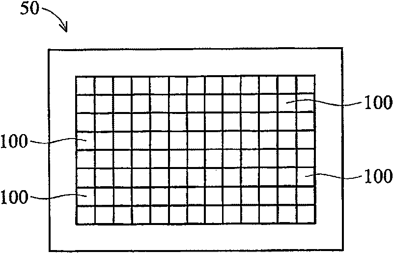
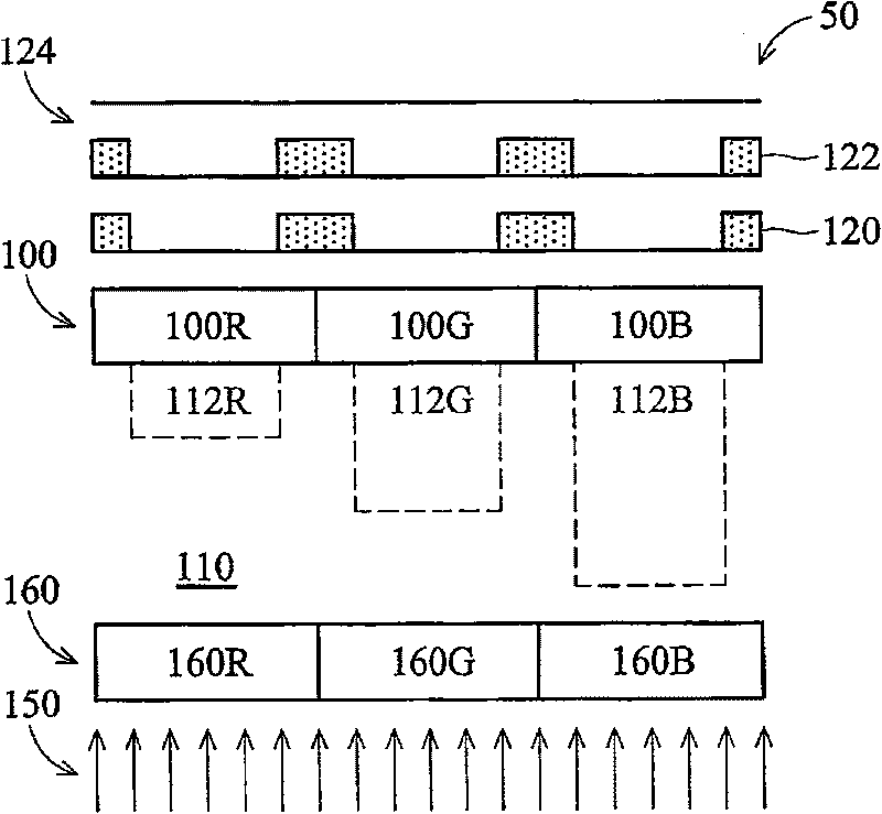
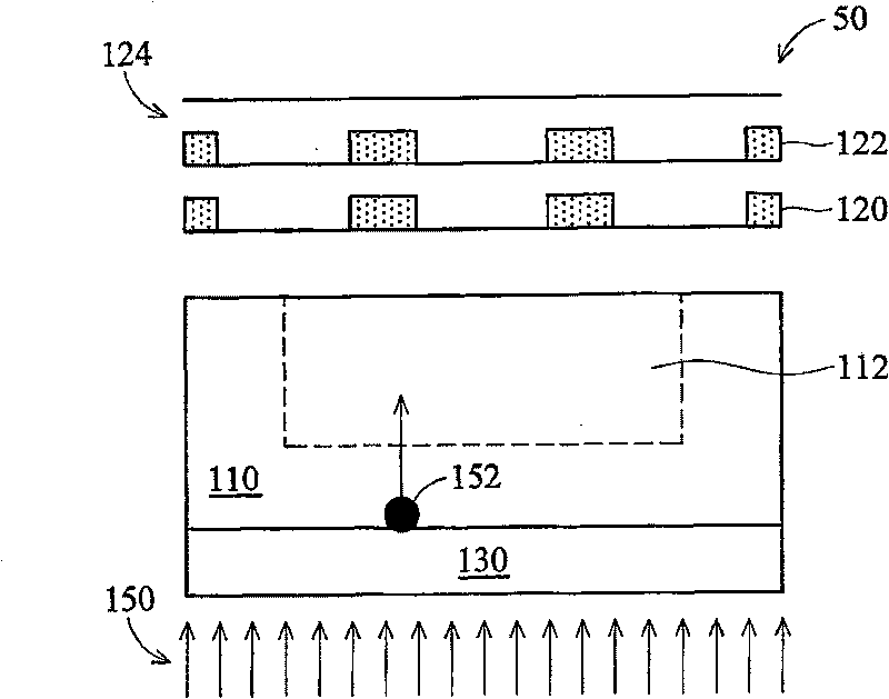
[0038] Please refer to figure 1 , an image sensor 50 provides a grid of backside illuminated pixels 100 . In this embodiment, the pixel 100 is a photosensitive diode or a photodiode, which is used to record the light intensity or ...


PUM


Abstract

The invention discloses a backside illuminated image sensor and a method for producing the backside illuminated image sensor. The method for producing the backside illuminated image sensor comprises asubstrate is provided; and the substrate is provided with a first conductive type and a first potential. A depletion region having a second conductivity type is formed within the substrate. The depletion region is extended. The thickness of the substrate is reduced. An ion having the first type and the second potential are implanted at the backside surface of the substrate to form a doping layer.A laser annealing on the doping layer is performed to activate the ion having the first type. The invention is characterized in that the thickness of the P- substrate is reduced before injecting a P+ion at backside surface of the P- substrate, so as to form a shallow P+ layer which provides an electric connection and decreases the leak current; besides, the laser annealing is performed to activate the injected ion, which has no influence on the metallic layer of the sensor, so that the luminous sensitivity can be improved without influencing the effect of the device and considering no extenal diffusion.

Description

technical field [0001] The invention relates to an optoelectronic device, in particular to a back-illuminated image sensing device with improved sensitivity and a manufacturing method thereof. Background technique [0002] Image sensors provide a grid of pixels to record the brightness or intensity of light, such as photodiodes or photodiodes, reset transistors (reset transistors), source follower transistors (source follower transistors), pinned photodiodes (pinned layer photodiode), and / or transfer transistor (transfer transistor). The pixel reacts to light by accumulating charges (the more light, the higher the charge). This charge can then be used by other circuits to provide color and brightness to suitable products, such as digital cameras. Common types of pixel grids include charge-coupled device (CCD) or complementary metal oxide semiconductor (CMOS) image sensors. [0003] Back-illuminated sensors are used to sense the amount of light projected onto the back surf...

Claims


Application Information

Patent Timeline
Patent Type & Authority Patents(China)
IPC IPC(8): H01L27/146H01L21/822
CPCH01L27/14621H01L27/14603H01L27/14683H01L27/1464
Inventor 许慈轩杨敦年
Owner TAIWAN SEMICON MFG CO LTD
Learn More