
Method of curing hydrogen silses quioxane and densification in nano-scale trenches

A hydrogen silsesquioxane, densification technology, applied in nanotechnology, semiconductor/solid-state device manufacturing, electrical components, etc., can solve problems such as difficult to fill trenches

Inactive Publication Date: 2008-05-21
DOW CORNING CORP
View PDF6 Cites 3 Cited by
  • Summary
  • Abstract
  • Description
  • Claims
  • Application Information

AI Technical Summary

Problems solved by technology

However, the disadvantage of the CVD method may be that it is difficult to adequately fill the trenches when their depth dimensions approach the sub-micron scale
Therefore CVD technology is not suitable for the nanoscale trench filling with high aspect ratio of the present invention

Method used


Image

  • Method of curing hydrogen silses quioxane and densification in nano-scale trenches
  • Method of curing hydrogen silses quioxane and densification in nano-scale trenches
  • Method of curing hydrogen silses quioxane and densification in nano-scale trenches

Examples


Embodiment 1

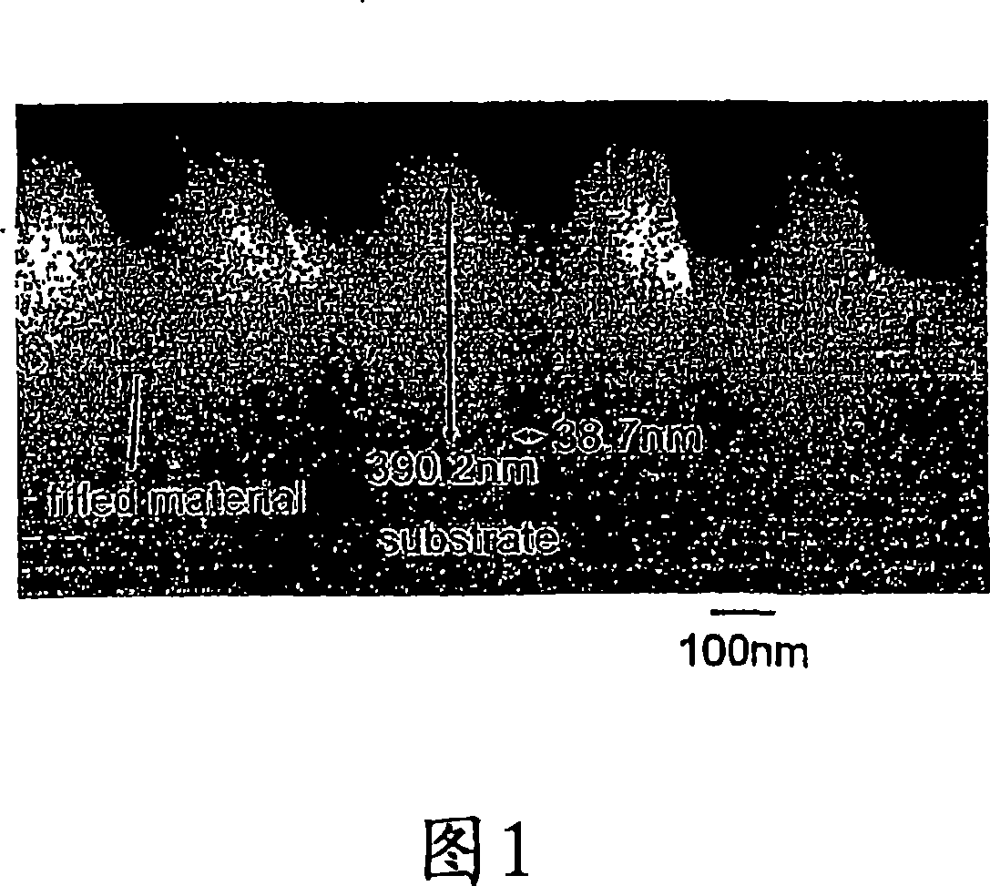
[0029] Two finely filtered HSQ solutions containing 4wt% and 8wt% HSQ in octamethyltrisiloxane were used. The film is spin-coated on the surface of the silicon wafer. In the first low temperature curing step, the film was initially kept at 100°C for 30 minutes in a water vapor environment. In the second low-temperature curing step, the temperature was increased to 250°C over 1 hour in a water vapor environment. During these two low temperature curing steps, water vapor remains in the grooves and reacts with HSQ. Then, in the third high temperature curing step, the film is further cured at 800° C. for 1 hour in a water vapor or nitrous oxide environment. The film was etched by exposing the film to a 200:1 hydrofluoric acid aqueous solution for 60 seconds, and the film loss was measured. The resulting film is shown in FIG. 1.

Embodiment 2

Example 2-Comparison

[0030] Example 1 was repeated at 800°C using normal oxidative curing but without water vapor. The etching resistance of the film was not observed. The filling material in the trench is completely removed.

Embodiment 3

[0031] Repeat Example 1, and nitrous oxide (N 2 O) Under the environment, further densify the cured HSQ film in the nano-scale trench of the silicon wafer. In particular, different temperatures were used to measure the curing of the HSQ resin film coated on the silicon wafer in a nitrous oxide environment. Using the same HF etching process as described in Example 1, the wet etching resistance in the nano-scale trench was measured. The process time for each measurement is 1 hour. As shown in Table 1, compared with the HSQ film cured in an oxygen or nitrogen environment, the film loss of the HSQ film cured in nitrous oxide is reduced in the dilute HF solution. In particular, at 800°C, the HSQ film cured under nitrous oxide has a film loss equivalent to that of a thermal oxide film. The values ​​of the thermal oxide film in Table 1 are published data in the literature. Table 1 also shows the increase in mechanical properties (ie, hardness and modulus) of the HSQ film cured under nitr...


PUM


Abstract

Trenches in a semiconductor substrate are filled by (i) dispensing a film forming material on the semiconductor substrate and into the trenches; (ii) curing the dispensed film forming material in the presence of an oxidant at a first low temperature for a first predetermined period of time; (iii) curing the dispensed film forming material in the presence of an oxidant at a second low temperature for a second predetermined period of time; (iv) curing the dispensed film forming material in the presence of an oxidant at a third high temperature for a third predetermined period of time; and (v) forming filled oxide trenches in the semiconductor substrate. The film forming material is hydrogen silsesquioxane.

Description

[0001] Cross reference of related applications [0001] no Invention field [0002] A method of curing hydrogen silsesquioxane (HSQ) in nano-scale trenches with high aspect ratio. High aspect ratio generally refers to narrow and deep grooves. Relative to the groove depth, the narrower the groove width, the higher the aspect ratio. The curing technology involves a three-stage process in the presence of oxidants such as water vapor and / or nitrous oxide in three different temperature ranges. Background of the invention [0003] Integrated circuit technology uses narrow trenches on semiconductor substrates to isolate circuits such as pre-metal dielectric (PMD) and shallow trench isolation (STI). The insulating material is deposited in the trench to form an insulating layer and planarize the topography. Chemical vapor deposition (CVD) and spin-on-glass deposition (SOD) are typically used to fill trenches on semiconductor substrates to form a dielectric layer, such as silicon dioxide (Si...

Claims


Application Information

Patent Timeline
Patent Type & Authority Applications(China)
IPC IPC(8): H01L21/762
CPCH01L21/02337H01L21/02134H01L21/316H01L21/3124H01L21/02282H01L21/02164H01L21/762B82Y40/00
Inventor 陈伟B·K·黄J-K·李E·S·梅尔M·J·斯波尔丁S·王
Owner DOW CORNING CORP
Learn More