Low etching photoresist cleaning agent and its cleaning method

A technology of photoresist and cleaning agent, which is applied in the fields of optics, photomechanical equipment, and photosensitive material processing, etc. It can solve the problems of semiconductor wafer substrate corrosion and other problems, and achieve the effect of obvious corrosion, strong cleaning ability, and reduced corrosion

Inactive Publication Date: 2008-05-28
ANJI MICROELECTRONICS (SHANGHAI) CO LTD
View PDF4 Cites 23 Cited by
  • Summary
  • Abstract
  • Description
  • Claims
  • Application Information

AI Technical Summary

Problems solved by technology

Higher cleaning temperatures can cause corrosion of semiconductor wafer substrates

Method used


Image

  • Low etching photoresist cleaning agent and its cleaning method
  • Low etching photoresist cleaning agent and its cleaning method

Examples


Embodiment 1~22

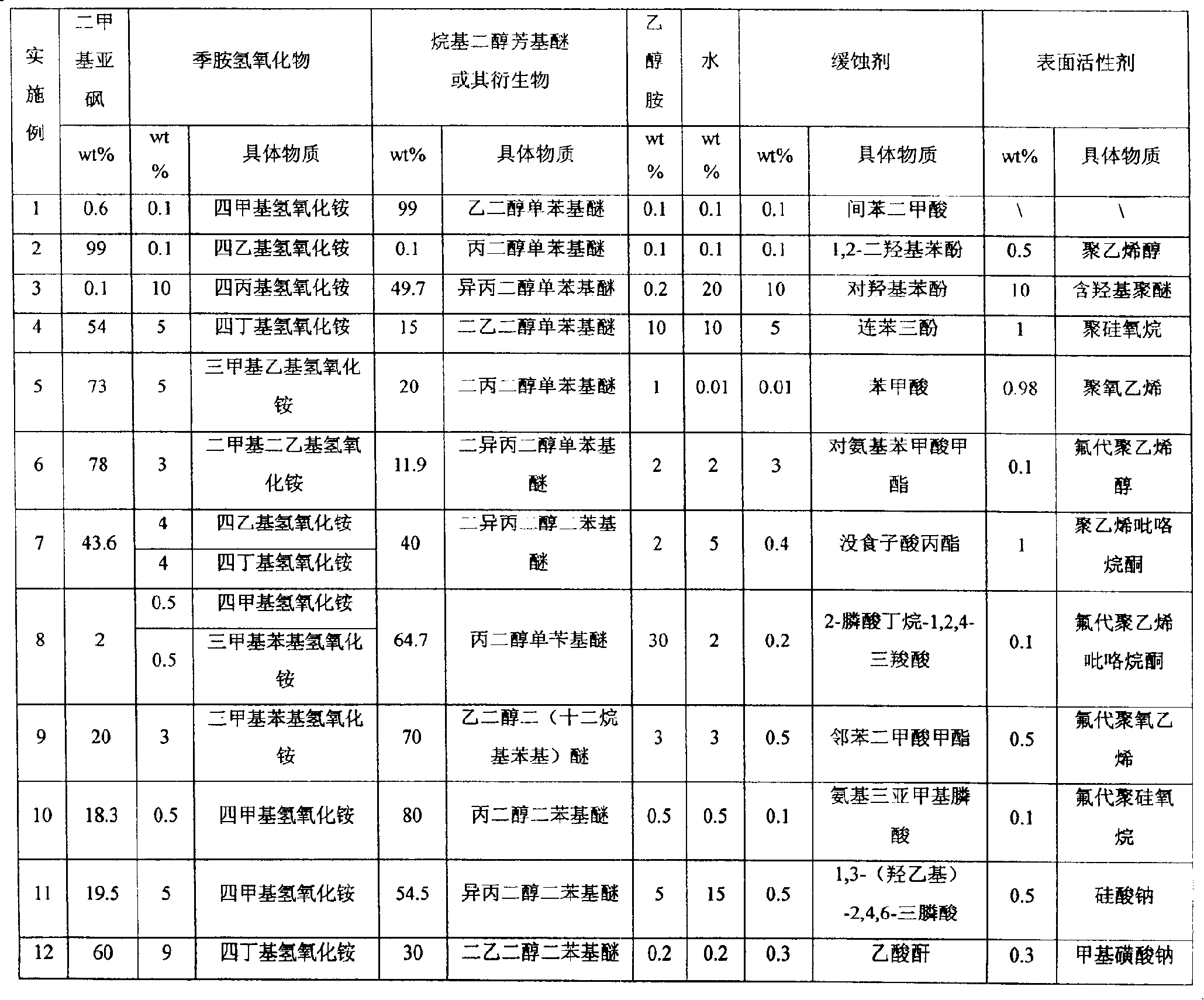
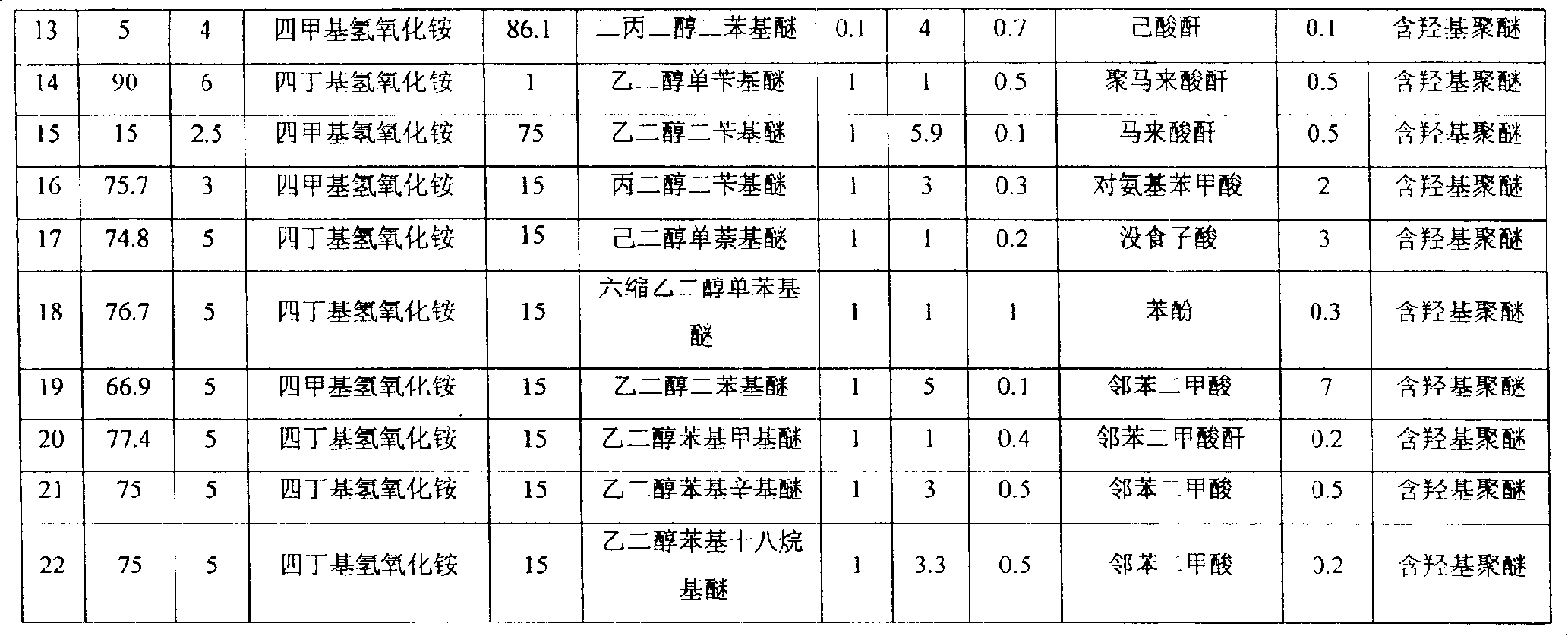
[0023] Embodiment 1~22 low etching property cleaning agent

[0024] Table 1 provides the composition formulations of the low-etching cleaning agent Examples 1-22. According to the formula in Table 1, the cleaning agent can be prepared by simply and uniformly mixing the components.

[0025] Table 1 Low Etching Cleaning Agent Example 1-22 Formula

[0026]

[0027]

Embodiment 1

[0042] Immerse the semiconductor wafer containing photoresist in a low-etching photoresist cleaning agent, wash it in batches at room temperature for 20 minutes, then wash it with deionized water, and then blow it dry with high-purity nitrogen.

Embodiment 2

[0044] Immerse the semiconductor wafer containing photoresist in a low-etching photoresist cleaning agent, clean it in batch rotation at 20°C for 30 minutes, then wash it with deionized water, and then blow it dry with high-purity nitrogen.


PUM


Abstract

The invention discloses a low-etching photoresist cleaning agent, which is characterized in that the invention comprises (a) quaternary ammonium hydroxide, (b) dimethyl sulfoxide, (c) alkyl glycol aryl ether and derivation of the alkyl glycol aryl ether whose molecular formula is like the indication of formula I, (d) aminoethyl alcohol, (e) water, (f) inhibitor, in the formula I, R1 chooses arylamine which contains 6 to 18 carbon atoms, m=2 to 6, n-1 to 6. The invention also provides a cleaning method for using the cleaning agent, which is characterized in that indoor temperature is less than 85 DEG C, a semiconductor crystal with photo resist is cleaned by low-etching photoresist cleaning agent, and then which is cleaned by deionized water, and is dried in nitrogen. The cleaning agent of the invention can be used for removing photo resist (light blockage) or other residues on metals, metal alloy, or dielectric substrate. The cleaning agent has strong cleaning ability, which has an obvious effect of corrosion inhibition to metals such as earth silicon, copper, phosphorus, and stannum and low K dielectric material and the like, and no black dots can be guaranteed, and the invention has a good application prospect in the microelectron field such as the cleaning of semiconductor crystal and the like.

Description

technical field [0001] The invention relates to a low-etching photoresist cleaning agent and a cleaning method thereof. Background technique [0002] In the usual semiconductor manufacturing process, a photoresist mask is formed on the surface of metals such as silicon dioxide, Cu (copper), and low-k materials, and pattern transfer is performed by wet or dry etching after exposure. Low temperature and fast cleaning process is an important direction for the development of semiconductor wafer manufacturing process. In addition, during the chemical cleaning process of the photoresist on the semiconductor wafer, the cleaning agent with a higher pH will cause corrosion of the wafer substrate. Especially in the process of using chemical cleaning agents to remove metal etching residues, metal corrosion is a common and very serious problem, which often leads to a significant decrease in wafer yield. [0003] The patent document WO04059700 utilizes an alkaline cleaning agent compos...

Claims


Application Information

Patent Timeline
Patent Type & Authority Applications(China)
IPC IPC(8): G03F7/42G03F7/32G03F7/26
CPCG03F7/425H01L21/31133G03F7/426
Inventor 刘兵彭洪修史永涛曾浩
Owner ANJI MICROELECTRONICS (SHANGHAI) CO LTD
Why Eureka
Try Eureka