Wafer press welding and bonding method and structure thereof

A bonding structure and wafer technology, applied in the direction of semiconductor/solid-state device parts, semiconductor devices, electrical components, etc., can solve the problem of wafers being easily broken, and achieve the effects of being beneficial to handling, increasing redundancy, and reducing costs

Active Publication Date: 2008-06-11
SEMICON MFG INT (SHANGHAI) CORP +1
View PDF1 Cites 35 Cited by
  • Summary
  • Abstract
  • Description
  • Claims
  • Application Information

AI Technical Summary

Problems solved by technology

[0013] Therefore, the object of the present invention is to provide a wafer bonding method and structure thereof, to solve the problem that wafers are easily broken in the existing wafer bonding process

Method used


Image

  • Wafer press welding and bonding method and structure thereof
  • Wafer press welding and bonding method and structure thereof
  • Wafer press welding and bonding method and structure thereof

Examples


Embodiment Construction

[0046] In order to make the above objects, features and advantages of the present invention more comprehensible, specific implementations of the present invention will be described in detail below in conjunction with the accompanying drawings.

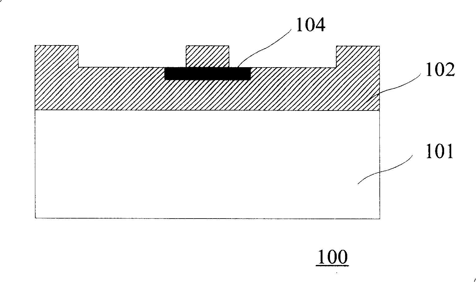
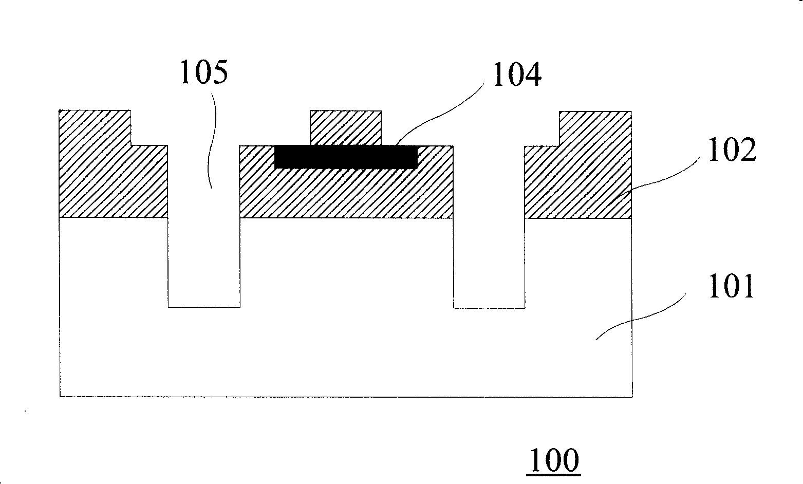
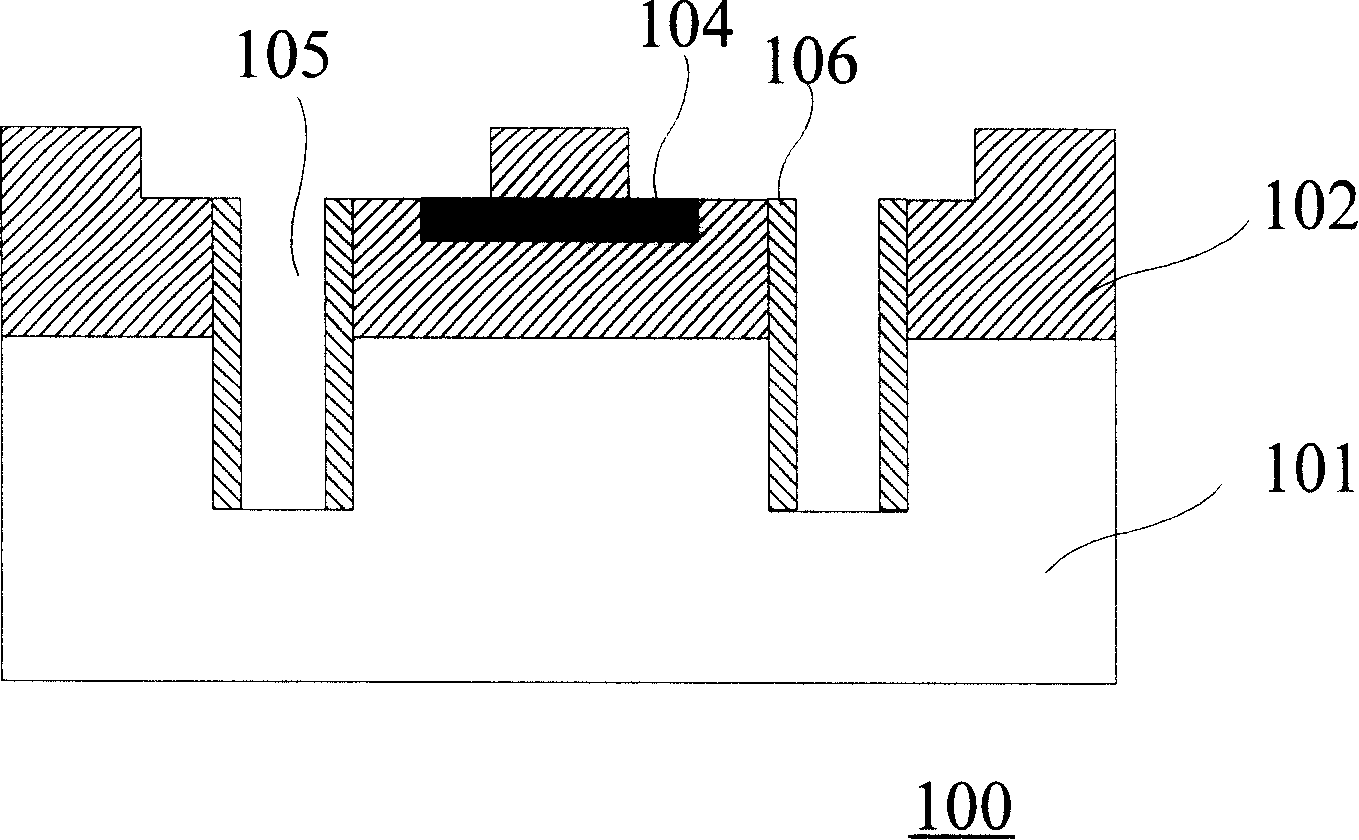
[0047] Figure 11 It is a flow chart of the wafer pressure bonding method of the present invention. Such as Figure 11 As shown, firstly, a first semiconductor wafer and a second semiconductor wafer are provided, the first semiconductor wafer and the second semiconductor wafer have completed chip manufacturing, and a passivation layer has been formed on the semiconductor wafer. The passivation layer is used to protect semiconductor chips and interconnection structures on the wafer from external moisture, scratches, and contamination. A first connection hole and a first groove are formed in the passivation layer of the first semiconductor wafer and the second semiconductor wafer by photolithography and etching process, and the bottom ...


PUM


Abstract

A three-dimensional interconnection method between wafers comprises the following steps that: firstly, two semiconductor wafers are bonded face to face, secondly the back of one of two semiconductor wafers is thinned to complete the three-dimensional interconnection between the wafers, thirdly the backs of the semiconductor wafers which complete interconnection are bonded spoon-fashion, thinned, and interconnected and the bonding spoon-fashion-thinning-interconnecting technique is repeated; the surfaces of a plurality of semiconductor wafers are overlaid in order. The invention also provides a three-dimensional interconnection structure between the wafers; the surfaces of two semiconductors are bonded face to face; a second connecting welding block is formed on a back underlay of one of the semiconductor wafers; a plurality of semiconductor wafers in order are overlaid on the semiconductor wafer underlay with the second connecting welding block. The method of the invention can not cause the damage to the wafer in a bonding process; a formed semiconductor wafer bonding structure can save the chip area of the semiconductor wafer.

Description

technical field [0001] The invention relates to the technical field of semiconductor manufacturing, in particular to a wafer bonding method and structure thereof. Background technique [0002] In the traditional dicing and packaging method, after the semiconductor wafer is manufactured, each chip is separated from the wafer by dicing, and then each chip is packaged and wired. With the development of semiconductor technology towards higher technology nodes, the packaging technology of semiconductor chips has gradually developed from the original cutting and bonding packaging method to wafer level package (wafer level package). In the wafer-level packaging method, the entire wafer is used as the packaging object, and two or more wafers are directly bonded together by wafer bonding after the wafer is manufactured. Chinese patent application number 200410005400.8 discloses a method and structure of wafer level packaging. Figure 1 to Figure 10 It is a schematic cross-sectional ...

Claims


Application Information

Patent Timeline
Patent Type & Authority Applications(China)
IPC IPC(8): H01L21/60H01L25/00H01L25/065H01L23/488
CPCH01L2224/16145
Inventor 黄河高大为王津洲毛剑宏
Owner SEMICON MFG INT (SHANGHAI) CORP
Why Eureka
Try Eureka