Method for filling isolation plough groove

A technology for isolation trenches and filling methods, which is applied in the fields of electrical components, semiconductor/solid-state device manufacturing, circuits, etc., and can solve the problems of weak plasma energy, large difference in flatness between the edge area and the central area of ​​the wafer, and high difficulty in wafer planarization, etc. question

Active Publication Date: 2008-06-11
SEMICON MFG INT (SHANGHAI) CORP +1
View PDF1 Cites 8 Cited by
  • Summary
  • Abstract
  • Description
  • Claims
  • Application Information

AI Technical Summary

Problems solved by technology

Due to the energy difference between the plasma central region and the edge region, the plasma energy at the edge of the wafer is relatively weak. As the deposition and etching processes alternate, the material filled and etched away at the edge of the wafer is less than that of the wafer. ce

Method used


Image

  • Method for filling isolation plough groove
  • Method for filling isolation plough groove
  • Method for filling isolation plough groove

Examples


Embodiment Construction

[0026] In order to make the above objects, features and advantages of the present invention more comprehensible, specific implementations of the present invention will be described in detail below in conjunction with the accompanying drawings.

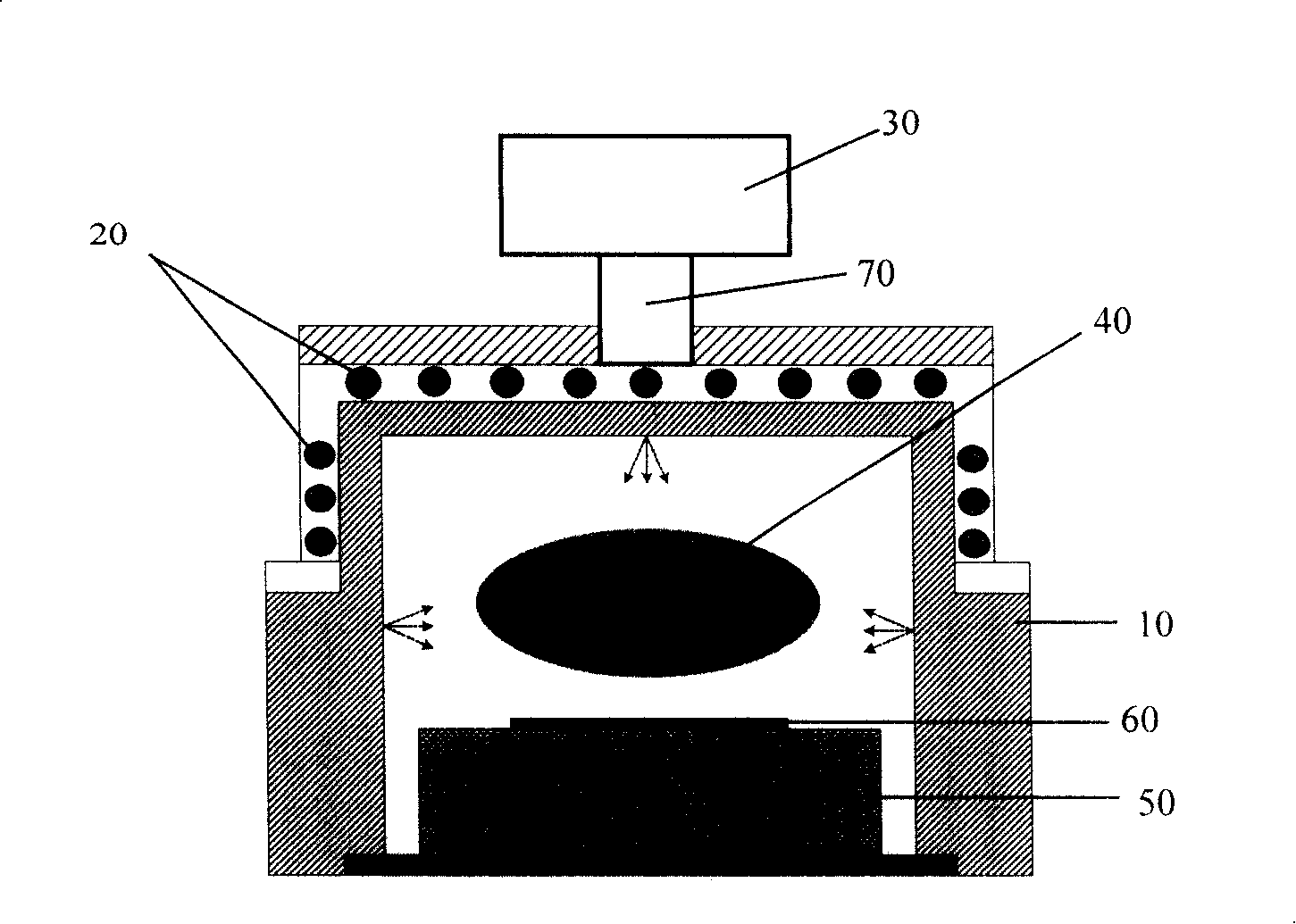
[0027] The invention relates to the technical field of semiconductor integrated circuit manufacturing, in particular to a method for filling isolation trenches in the manufacturing process of semiconductor devices. It should be noted here that this specification provides different embodiments to illustrate the various features of the present invention, but these embodiments are only for convenience of description by using specific compositions and structures, and do not limit the present invention.

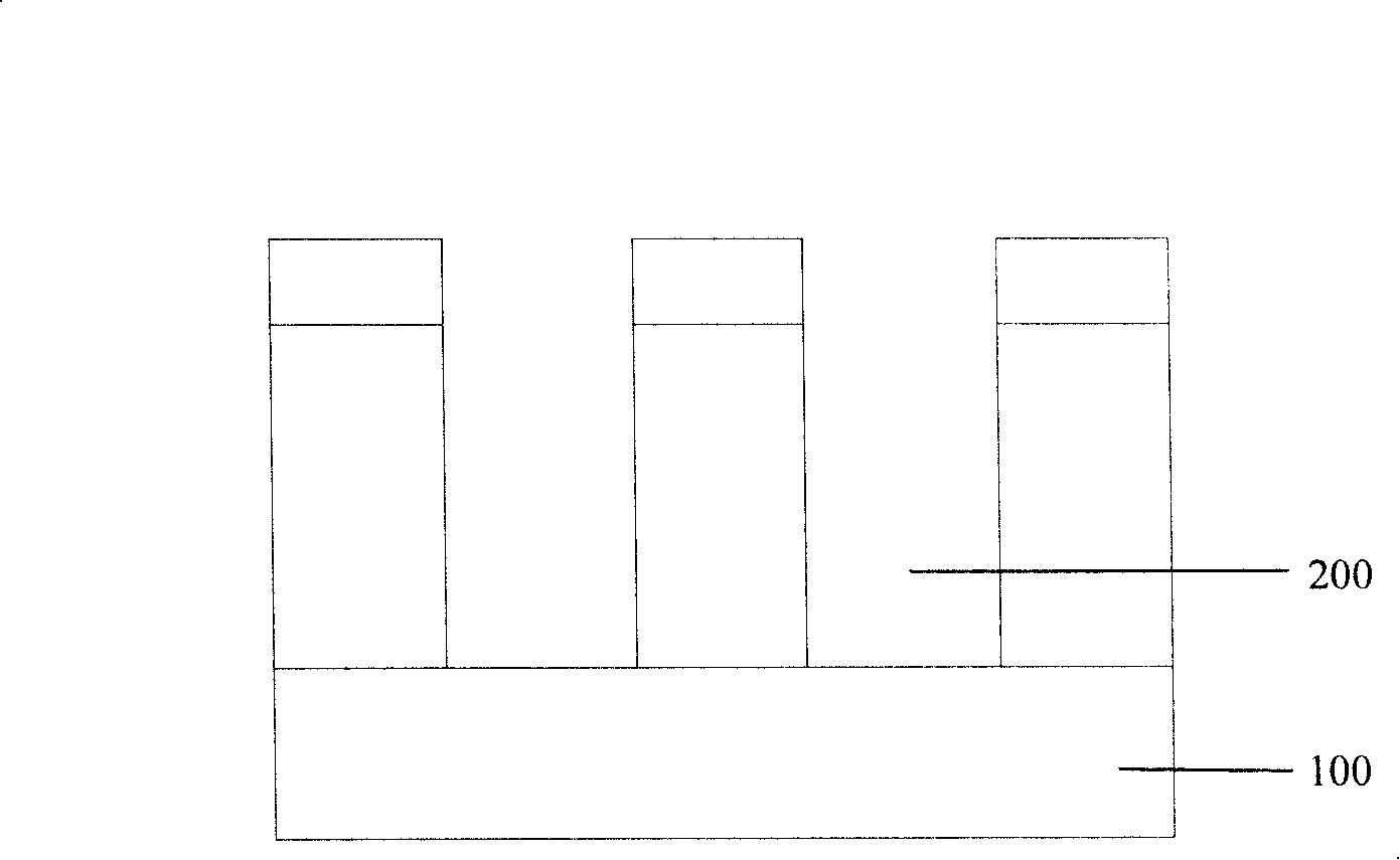
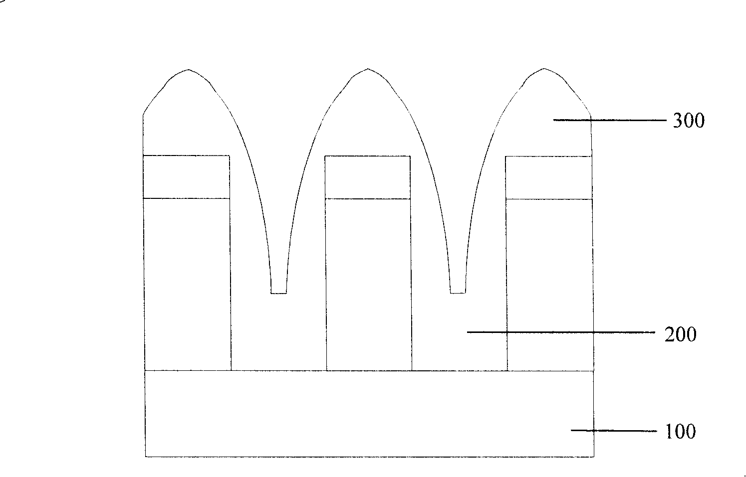
[0028] Due to the relatively high aspect ratio of deep submicron device trenches, it is usually greater than 4. Therefore, high-density plasma chemical vapor deposition (High-Density-Plasma CVD, HDP-CVD) plus in-situ etching process is use...


PUM


Abstract

The invention relates to an isolation groove filling method which comprises the following steps that: a semiconductor substrate is provided; the surface of the substrate is provided with an isolation groove; at least a high-density plasma chemical vapor deposition technique and at least an etching technique are performed; insulating substance is deposited on the groove till the groove is filled in; the high-density plasma chemical vapor deposition technique with a first sputtering yield is continued to perform; a covering layer is deposited on the surface of the insulating substance; the high-density plasma chemical vapor deposition technique with a second sputtering yield is performed; another covering layer is also deposited on the surface of the covering layer; the second sputtering yield is greater than the first sputtering yield. The isolation groove filling method of the invention can increase the thickness of the insulating layer on the fringe field of a wafer after the wafer with large dimension is filled in the isolation groove, thereby improving the consistency and flatness of the insulating layer thickness of the central field and the fringe field of the wafer.

Description

technical field [0001] The invention relates to the technical field of semiconductor manufacturing, in particular to a method for filling isolation trenches. Background technique [0002] Plasma is used extensively in semiconductor manufacturing processes. Plasma is usually generated in a low-pressure environment. The reaction gas is introduced into the reaction chamber and the electron flow is introduced, and the electrons are accelerated by a radio frequency (RF) electric field, so that the electrons collide with the gas molecules and transfer kinetic energy, thereby ionizing the gas molecules. become plasma. The generated plasma can be used in various semiconductor manufacturing processes, such as plasma etching, deposition, etc. European Patent Application No. 95307268.3 discloses a system for generating plasma, figure 1 A simplified schematic diagram of the existing system structure for generating plasma, such as figure 1 As shown, the system includes a reaction cha...

Claims


Application Information

Patent Timeline
IPC IPC(8): H01L21/762
Inventor 刘明源
Owner SEMICON MFG INT (SHANGHAI) CORP
Why Eureka
Try Eureka