Semiconductor device and its manufacturing method

A semiconductor and device technology, applied in the field of complementary metal oxide semiconductor devices and their manufacturing, can solve the problems of difficulty in space filling, narrow space distance between gates 12 and 14, deposition effect affecting the quality of the formation of contact holes 16, etc. Filling effect and coverage ability, improving device performance, reducing the effect of filling difficulty

Active Publication Date: 2008-06-11
SEMICON MFG INT (SHANGHAI) CORP +1
View PDF1 Cites 8 Cited by
  • Summary
  • Abstract
  • Description
  • Claims
  • Application Information

AI Technical Summary

Problems solved by technology

Since the PMD layer 20 needs to fill the space between the grid electrodes 14 and 12 without gaps, the deposition effect of the PMD layer 20 affects the formation quality of the follow-up contact hole 16
When the manufacturing process enters the process node below 90nm, the space distance between the gates 12 and 14 is very narrow, similar to a high aspect ratio trench. In this case, it becomes more and more difficult to fill the space between the gates 12 and 14. difficulty

Method used


Image

  • Semiconductor device and its manufacturing method
  • Semiconductor device and its manufacturing method
  • Semiconductor device and its manufacturing method

Examples


Embodiment Construction

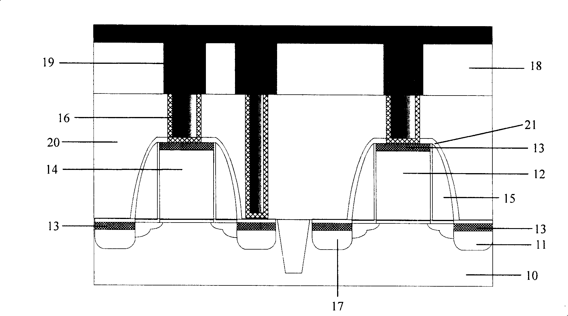
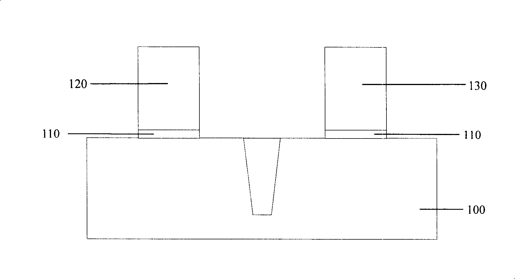
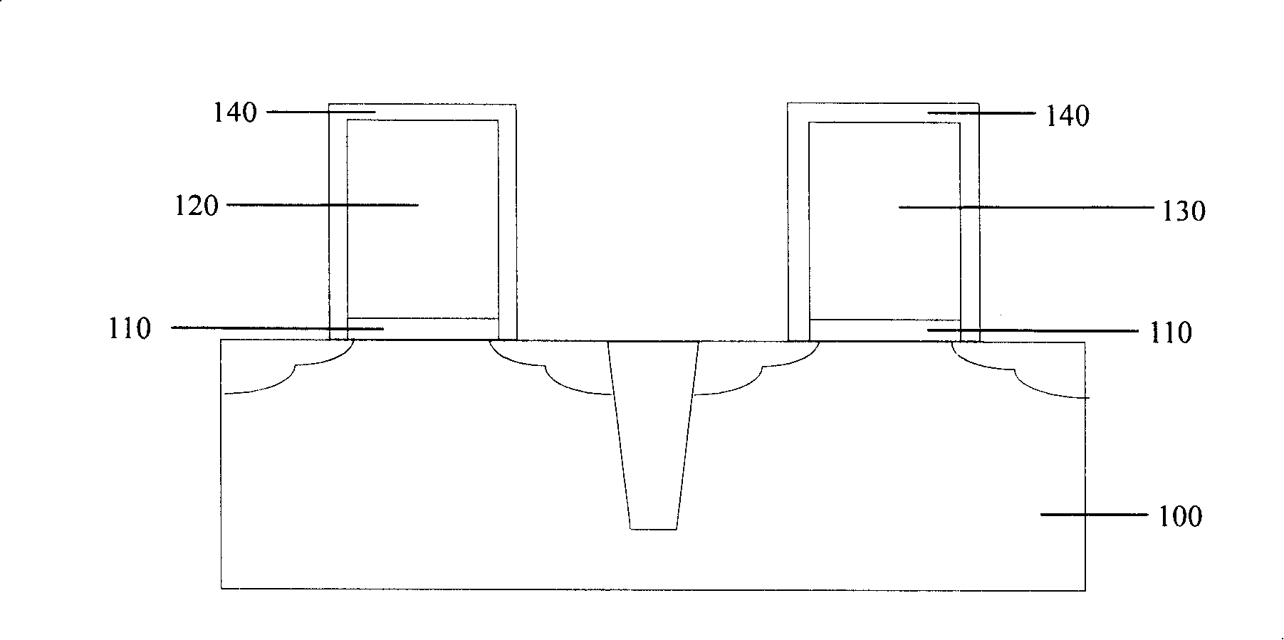
[0029] In order to make the above objects, features and advantages of the present invention more comprehensible, specific implementations of the present invention will be described in detail below in conjunction with the accompanying drawings.

[0030] In the following description, numerous specific details are set forth in order to provide a thorough understanding of the present invention. However, the present invention can be implemented in many ways other than those described here, and those skilled in the art can make similar extensions without departing from the connotation of the present invention. Accordingly, the invention is not limited to the specific implementations disclosed below.

[0031] Figure 2 to Figure 9 A cross-sectional schematic diagram illustrating a method for manufacturing a semiconductor device according to an embodiment of the present invention is merely an example, which should not limit the protection scope of the present invention excessively. ...


PUM


Abstract

The invention discloses a manufacturing method for a semiconductor device, including the following steps that: a grid electrode with a sidewall spacer is formed on a semiconductor substrate; the sidewall spacer comprises a silicon oxide layer and a silicon nitride layer; a source region and a drain region are formed inside the semiconductor substrate; moreover, metal silicides are formed on the surfaces of the grid electrode, the source region and the drain region; the silicon nitride layer arranged inside the sidewall spacer is removed; an etching stop layer is formed on the surface of the substrate comprising the grid electrode, the source region and the drain region; moreover, a medium layer is deposited on the surface of the etching stop layer. The invention can improve the filling quality of a PMD layer in the space between grid electrodes.

Description

technical field [0001] The invention relates to the technical field of semiconductor manufacturing, in particular to a complementary metal oxide semiconductor device (CMOS) and a manufacturing method thereof. Background technique [0002] With the rapid development of semiconductor device manufacturing technology, the density of devices in integrated circuits is getting higher and higher, and the critical dimensions of devices have reached the deep submicron stage. In this case, new challenges are presented for the space filling process between components. figure 1 A schematic diagram illustrating an existing semiconductor device and its formation process. Such as figure 1 As shown, at the beginning of the back end of line (BEOL) forming the interconnection layer, it is usually necessary to combine the MOS transistors formed in the front end of line (FEOL) with the lowest layer of the interconnection layer A dielectric layer 20 is deposited between the 18, and the dielect...

Claims


Application Information

Patent Timeline
Patent Type & Authority Applications(China)
IPC IPC(8): H01L21/8238H01L21/336H01L27/092H01L29/78
Inventor 宁先捷
Owner SEMICON MFG INT (SHANGHAI) CORP
Why Eureka
Try Eureka