CMOS-device and manufacture method of the cmos device
A technology for cooling components and image sensors, which is applied in the manufacture/processing of thermoelectric devices, semiconductor/solid-state device manufacturing, semiconductor/solid-state device components, etc., and can solve problems such as dark current problems
- Summary
- Abstract
- Description
- Claims
- Application Information
AI Technical Summary
Problems solved by technology
Method used
Image

Examples
Embodiment Construction
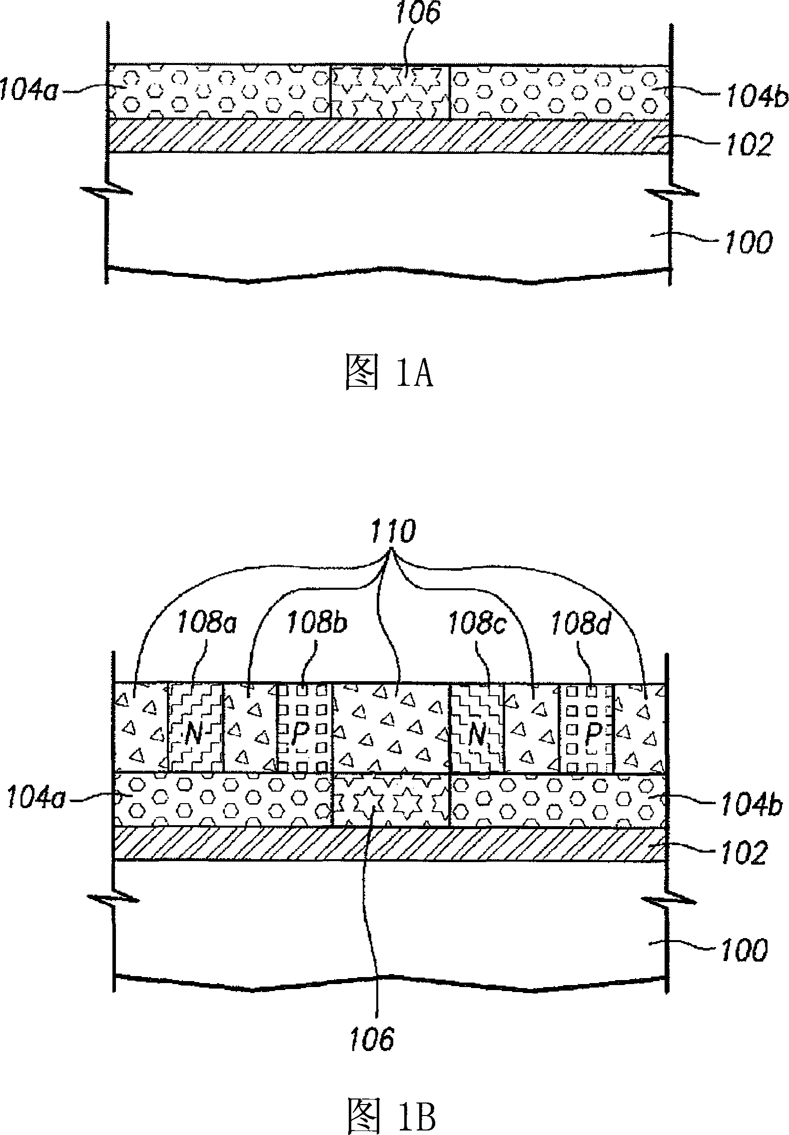
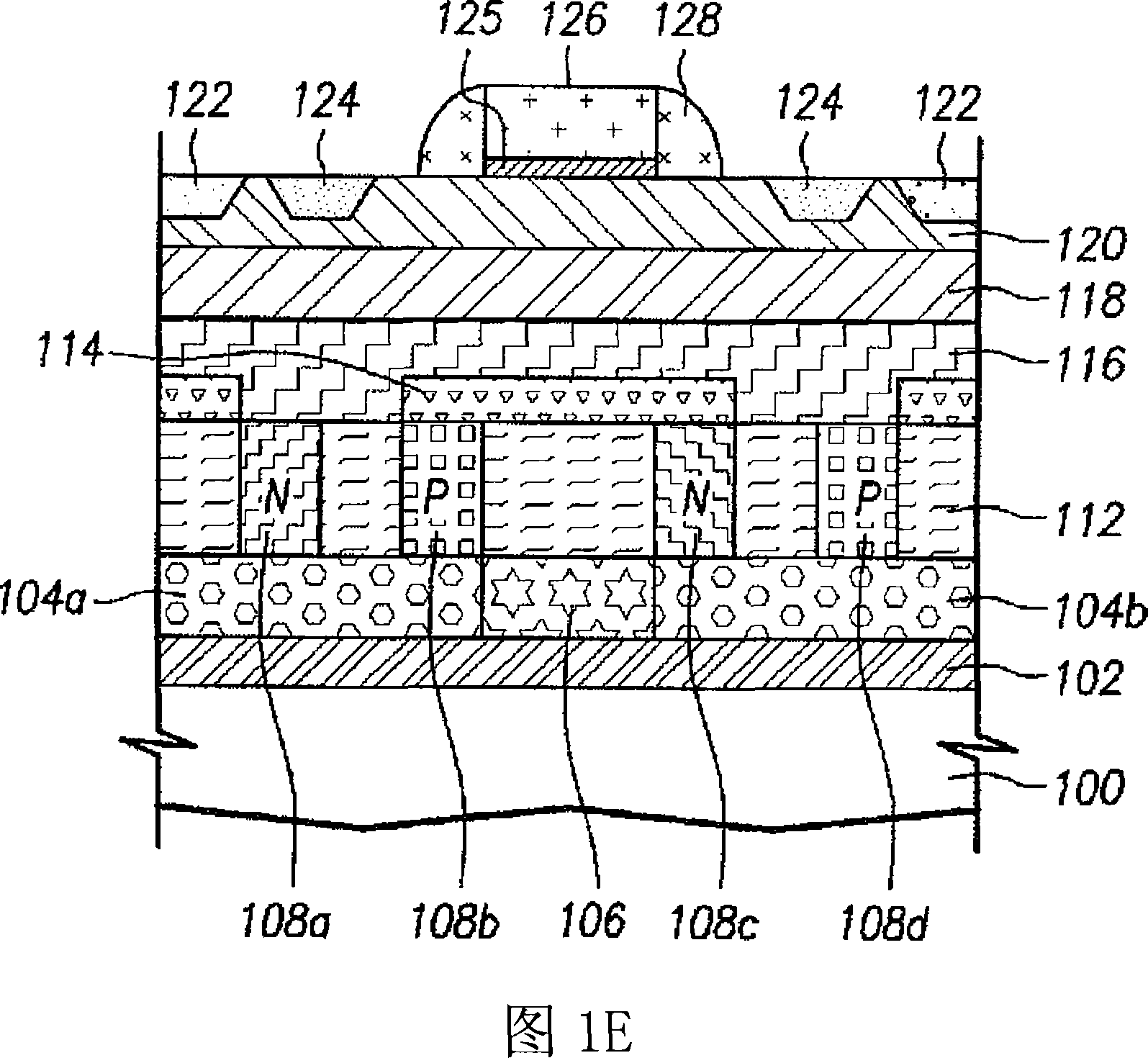
[0015] As shown in the embodiment of FIG. 1A , the first insulating film 102 and the first polysilicon film may be sequentially deposited with a predetermined thickness on or over the underlying substrate 100 . The lower substrate 100 may be formed of a heat sink or a polysilicon film. The first insulating film 102 can be made of silicon oxide film (SiO 2 ) or aluminum oxide films. The first insulating film 102 may have a thickness ranging from 10 to 300 μm.
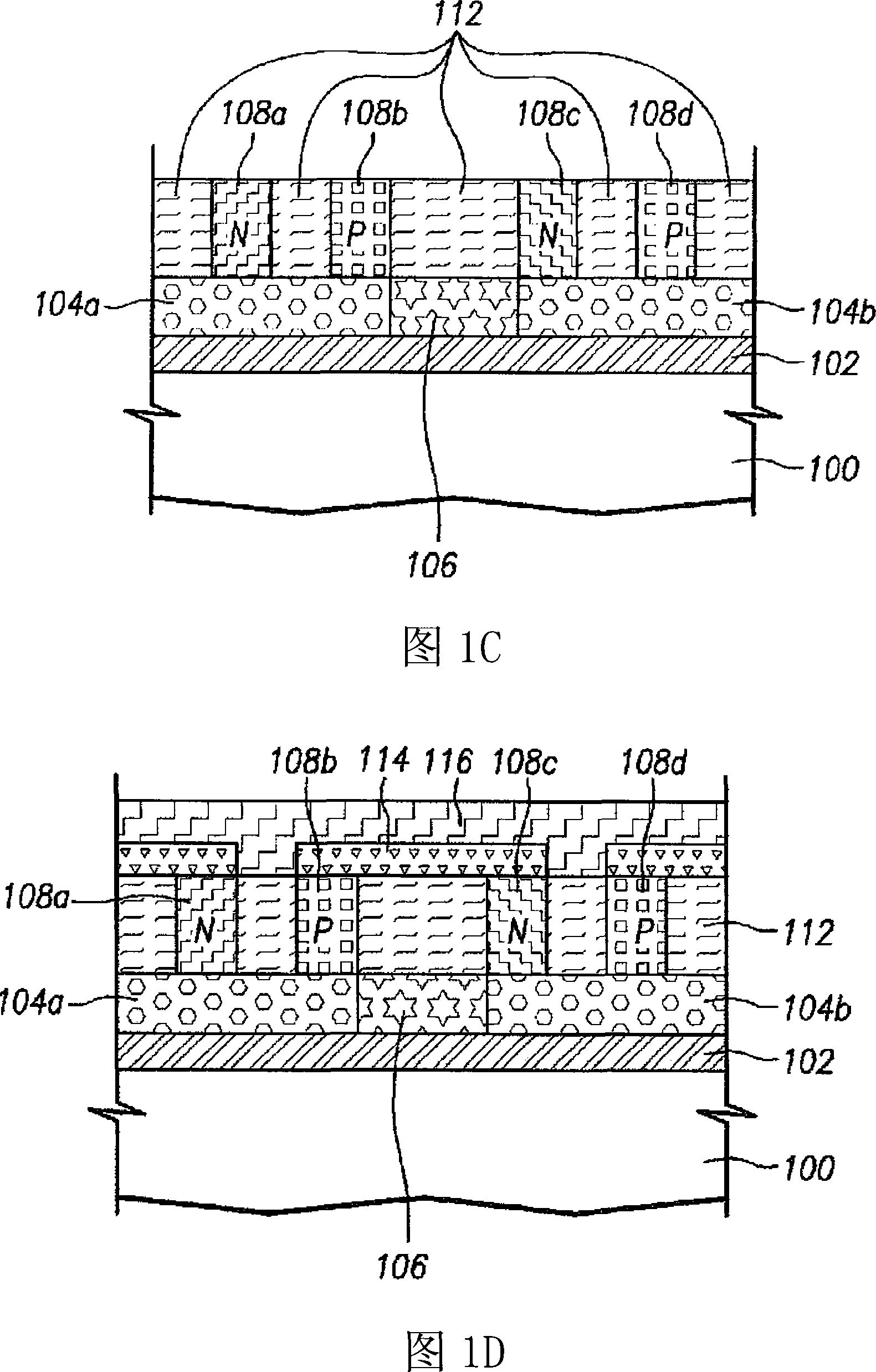
[0016] Thereafter, a first photoresist pattern may be formed on or over the first polysilicon film. Subsequently, an ion implantation process is performed using the first photoresist pattern as a mask, thereby implanting dopant ions into the first polysilicon film to form the first lower layer conductor 104a, the second lower layer conductor 104b, and the first lower layer conductor 104b. The first region 106 is provided between the conductor 104a and the second lower conductor 104b. The first lower layer conductor 1...
PUM
 Abstract
Description
Claims
Application Information
 - R&D
- Intellectual Property
- Life Sciences
- Materials
- Tech Scout
- Unparalleled Data Quality
- Higher Quality Content
- 60% Fewer Hallucinations
Browse by: Latest US Patents, China's latest patents, Technical Efficacy Thesaurus, Application Domain, Technology Topic, Popular Technical Reports.
© 2025 PatSnap. All rights reserved.Legal|Privacy policy|Modern Slavery Act Transparency Statement|Sitemap|About US| Contact US: help@patsnap.com