Semiconductor device has conductive projection and its manufacturing method

A conductive bump and semiconductor technology, which is applied in semiconductor/solid-state device manufacturing, semiconductor devices, semiconductor/solid-state device components, etc., can solve the cracking and delamination of the metal layer at the bottom of the solder bump, and the ineffectiveness of the metal layer at the bottom of the solder bump. Absorb copper pillar stress and other issues

Inactive Publication Date: 2008-07-16
SILICONWARE PRECISION IND CO LTD
View PDF7 Cites 6 Cited by
  • Summary
  • Abstract
  • Description
  • Claims
  • Application Information

AI Technical Summary

Problems solved by technology

[0005] Although the aforementioned conductive bumps with relatively high height copper pillars can absorb large thermal stress (thermal stress) when the thermal expansion coefficient difference between the chip and the substrate is large, but when applied to a chip with a larger size, such as 15*15mm In the above, for the conductive bumps containing copper pillars formed at the corners of the chip, because the thermal stress it receives is farther away from the center of the chip, the thermal stress it bears is relatively greater, which leads to the metal layer at the bottom of the solder bump It is still unable to effectively absorb the stress transmitted by the copper pillar, and the cracking and delamination C problems of the metal layer at the bottom of the solder block are still very easy to occur here, such as Figure 1B shown

Method used


Image

  • Semiconductor device has conductive projection and its manufacturing method
  • Semiconductor device has conductive projection and its manufacturing method
  • Semiconductor device has conductive projection and its manufacturing method

Examples


no. 1 example

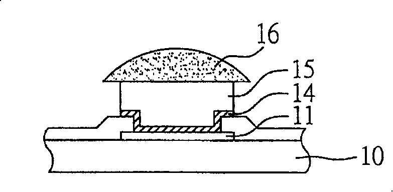
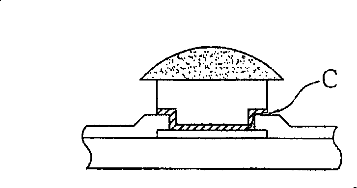
[0077] see Figure 2A to Figure 2F , is a schematic cross-sectional view showing the first embodiment of the semiconductor device with conductive bumps and its manufacturing method of the present invention.

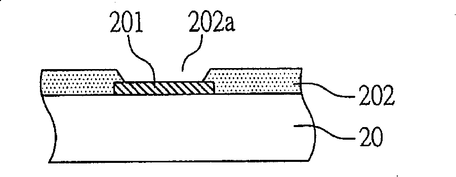
[0078] Such as Figure 2A As shown, firstly, a semiconductor base material 20 with a plurality of welding pads 201 and a protective layer 202 is prefabricated on the surface (in this figure, only the area covered by a single welding pad 201 is illustrated), and the semiconductor base material is, for example, a semiconductor A chip or wafer comprising a plurality of chip units. The semiconductor substrate 20 is covered with a protective layer 202, and the protective layer 202 has an opening 202a to expose the pad 201. The material of the protective layer 202 is, for example, polyimide (PI) to protect the semiconductor substrate. 20.

[0079] Such as Figure 2B As shown, the first metal layer 241 is directly formed on the semiconductor substrate 20 , and the first meta...

no. 2 example

[0093] see image 3 , is a schematic cross-sectional view of the second embodiment of the semiconductor device with conductive bumps of the present invention. The semiconductor device with conductive bumps in this embodiment is roughly the same as the previous embodiment, and the main difference is that when the protective layer material of the semiconductor substrate is such as When it is a nitride (such as silicon nitride), a first covering layer can be covered on the protective layer first, and then a first metal layer, a second covering, a second metal layer, and a second metal layer are sequentially formed on the first covering layer. The third covering layer, the metal post and the solder material.

[0094] As shown in the figure, the first covering layer 331 covers the protective layer 302 of the semiconductor substrate 30 and exposes the solder pad 301. The first covering layer 331 can be selected from benzo-cyclobutene (Benzo-Cyclo- One of Butene; BCB) and polyimide ...

no. 3 example

[0097] see Figure 4 , is a schematic cross-sectional view of the third embodiment of the semiconductor device with conductive bumps of the present invention, the semiconductor device with conductive bumps of this embodiment is roughly the same as the first embodiment, the main difference is that a solder pad 401 is provided on the surface A first metal layer 441, a second covering layer 432, and a second metal layer 442 are successively formed on the semiconductor substrate 40 of the protective layer 402, and the second metal layer 442 is electrically connected to the first metal layer 441, Then cover the third covering layer 433 on the second metal layer 442 and the second covering layer 432, and make the third covering layer 433 correspond to the position vertically above the welding pad 401 to be provided with an opening 433a, exposing part of the first Two metal layers 442 .

[0098] Next, a third metal layer 443 is formed on the second metal layer 442 exposing the openi...


PUM


Abstract

The invention discloses a semiconductor device with a conductive lug and a method for preparing the same, wherein the method mainly is that: a first metal layer electrically connected with the welding pad is formed on a semiconductor base material with a welding pad and a protective layer and is covered with and partially exposed from a second covering layer; and a second metal layer which is in electric connection with the first metal layer form the exposed part is formed on the second covering layer, and is covered with and is exposed partially from an opening of a third covering layer, and a conductive bump having a metal column and a soldering tin material is formed on the second metal layer in the opening accordingly, thereby providing a buffer effect by means of the covering layers and the metal layers and avoiding the problem of layer separation because the prior under bump metallurgy of a welding block formed on the welding pad directly withstands the stress transmitted by the metal column.

Description

technical field [0001] The invention relates to a semiconductor device and its manufacturing method, in particular to a semiconductor device with conductive bumps and its manufacturing method. Background technique [0002] The traditional flip-chip (Flip Chip) semiconductor packaging technology is mainly to form solder bumps (Solder Bump) on the pads of the chip, and then directly electrically connect with the carrier such as the substrate (Substrate) through the solder bumps. In terms of wire bonding, flip-chip technology has a shorter circuit path and better electrical quality. At the same time, it can be designed in the form of an exposed crystal back, which can also improve chip heat dissipation. [0003] Before forming solder bumps on the chip with the flip-chip technology, it is necessary to form the Under Bump Metallurgy (UBM) on the chip pads as disclosed in US Patent Nos. 6,111,321, 6,107,180, and 6,586,323. , so that the solder bumps can be firmly adhered to the c...

Claims


Application Information

Patent Timeline
Patent Type & Authority Applications(China)
IPC IPC(8): H01L21/60H01L23/485
CPCH01L24/11H01L2224/11H01L2224/13H01L2224/13082H01L2224/131H01L2224/13562H01L2224/136H01L2924/351H01L2924/00H01L2924/014H01L2924/00012
Inventor 柯俊吉黄建屏
Owner SILICONWARE PRECISION IND CO LTD
Why Eureka
Try Eureka